🧬 Professor Giriraja C. V.'s Exam Pattern DNA
50-Mark BlueprintBased on the official September 2026 examination paper, here is the exact question structure and marking formula:
| Question Type & Marks | Topics Tested | Evaluation Criteria (How to Get 50/50) |
|---|---|---|
| Part 1: Theory & Advantages [5M] (Q1: BTL1) |
Cortex-M Processor Family Advantages, Architecture overview. | List 5 crisp points from 1 23ECE313_ES_Ch4 Text 1.pdf (Low power/WIC, Thumb-2, NVIC 12-cycle latency, OS support with MSP/PSP, CoreSight debug). |
| Part 2: Assembly & Stack Trace [5M] (Q2: BTL2) |
Instruction execution (LDR, MOVS flags, IT blocks, STMDB/LDMIA, Full Descending Stack, ICI bits). | Calculate exact register hex values, draw 4-byte memory map addresses, explain EPSR ICI bits preventing multi-cycle restart. |
| Part 3: Hardware Interfacing [5M] (Q3: BTL2) |
JTAG vs SWD, CoreSight host connection, SWJ-DP, DAP, AHB-AP. | Draw host-to-core DAP interconnect diagram from 5 23ECE313_ES_Ch15_Txt 1a.pdf. Explain non-intrusive memory access while CPU runs. |
| Part 4: Timing Waveforms [15M] (Q4, Q5, Q6: 5M each, BTL2) |
1. SysTick task switching timeline. 2. Interrupt pending & activation state machine. 3. Context switch IRQ blocking & PendSV solution. |
"With the help of a neat timing diagram" is mandatory. Must draw the exact waveforms from Ch12 and Ch_Txt1 slides with timeline states. |
| Part 5: Low Power / Core Feature [5M] (Q7: BTL2) |
Wake-Up Interrupt Controller (WIC) in Deep Sleep, Sleep-on-Exit. | Draw WIC always-on power domain block diagram and list the 7-step sequence of events restoring CPU clocks. |
| Part 6: Applied Coding & Circuit [15M] (Q8: 5M + Q9: 10M, BTL3) |
• Q8: PWM Duty Cycle control (MOSFET, 3V from 5V DC). • Q9: Analog sensor (PA0), Relay Fan (PA5), UART PuTTY display. |
Must draw both Circuit Diagram AND write complete C code with exact registers (MODER, AFR, ARR, CCR1, ADC1->SQR3, CR2, BRR). |
⚡ Unit II: Fault Exceptions, SVC & PendSV (OS Services)
High Weightage Theory1. PendSV & Deferred Context Switching (Guaranteed 8-Mark Diagram Question)
"Explain the need for Pendable Service Call (PendSV). Illustrate with timing diagrams why context switching inside a regular timer IRQ causes latency issues and how PendSV resolves it."
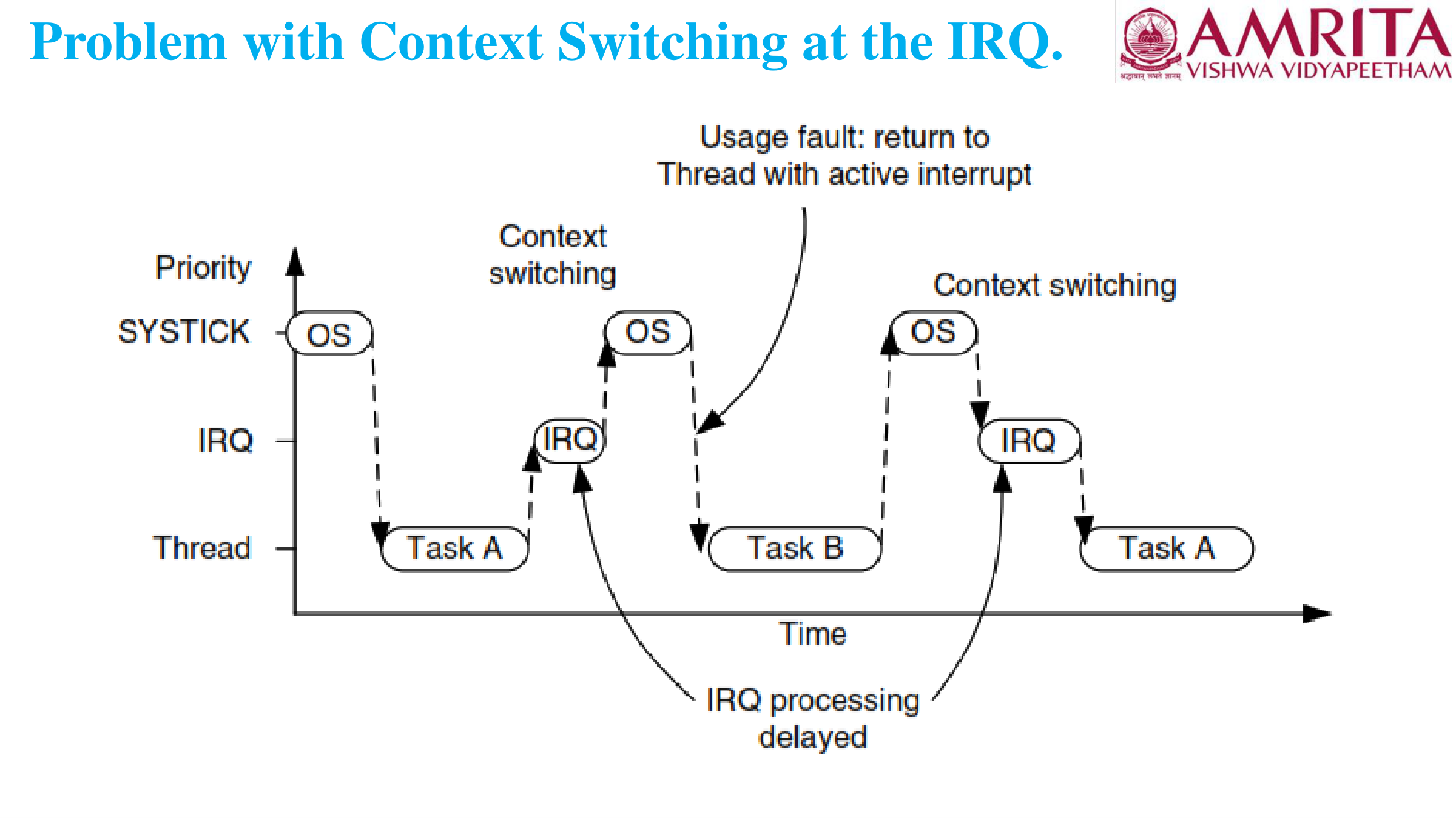
Detailed Step-by-Step Operation:
- Step 1 (Normal Execution): Task A is executing in Thread mode at the lowest logical priority.
- Step 2 (SysTick Trigger): Periodic SysTick interrupt fires. The CPU enters the SysTick handler in Handler mode to perform an OS context switch.
- Step 3 (The Conflict): An external peripheral interrupt (e.g., UART or Motor Control IRQ) arrives while the context switch is executing.
- The Failure: Because the SysTick ISR is actively executing, the peripheral IRQ is blocked and delayed until the entire lengthy context switch finishes. This leads to latency violations, jitter, and missed real-time deadlines in safety-critical systems!
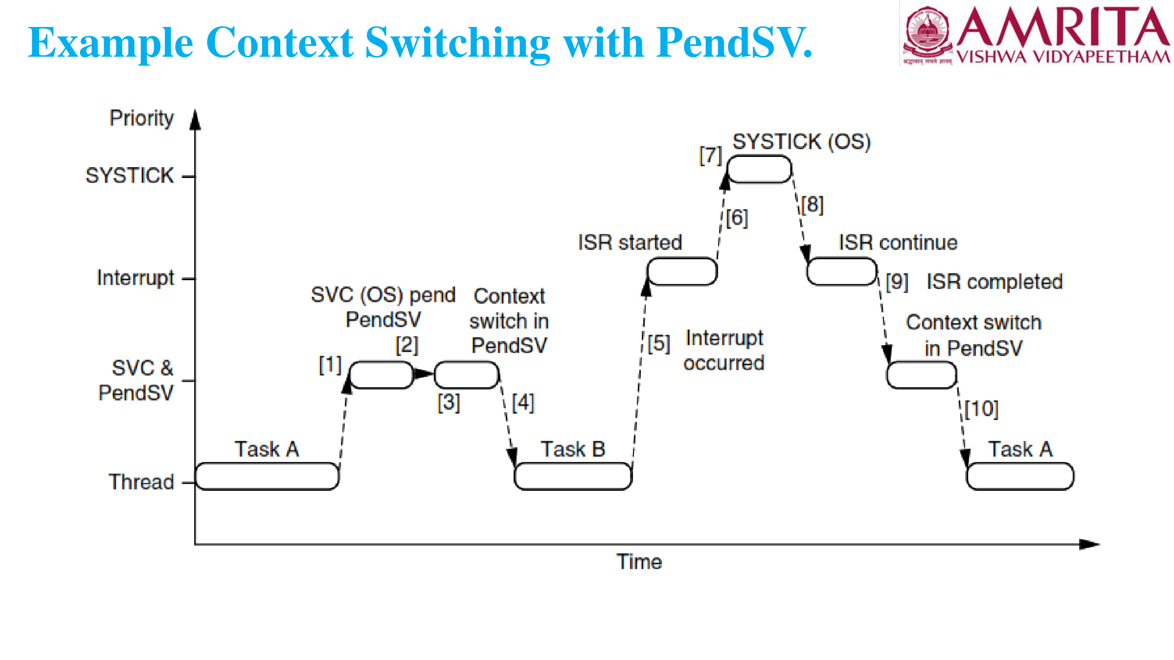
How PendSV Resolves the Latency Issue:
- Configuration: PendSV is programmed with the lowest priority level in the NVIC (via
SHPR3register). - Deferred Request: When SysTick decides a context switch is required, it does not perform the switch immediately. Instead, it simply sets the
PENDSVSETbit in the Interrupt Control and State Register (ICSR) and exits immediately. - Immediate Preemption: Because SysTick exits immediately, the pending high-priority peripheral IRQ executes with zero latency!
- Execution Point: PendSV executes only when all higher-priority ISRs have finished and returned. It then safely saves Task A\'s context and restores Task B\'s context without ever delaying hardware interrupts.
2. Supervisor Call (SVC) & Context Extraction
SVC #imm8 instruction causes Exception 11. It provides an architected gate for unprivileged user tasks to switch to privileged Handler mode to request operating system kernel services.
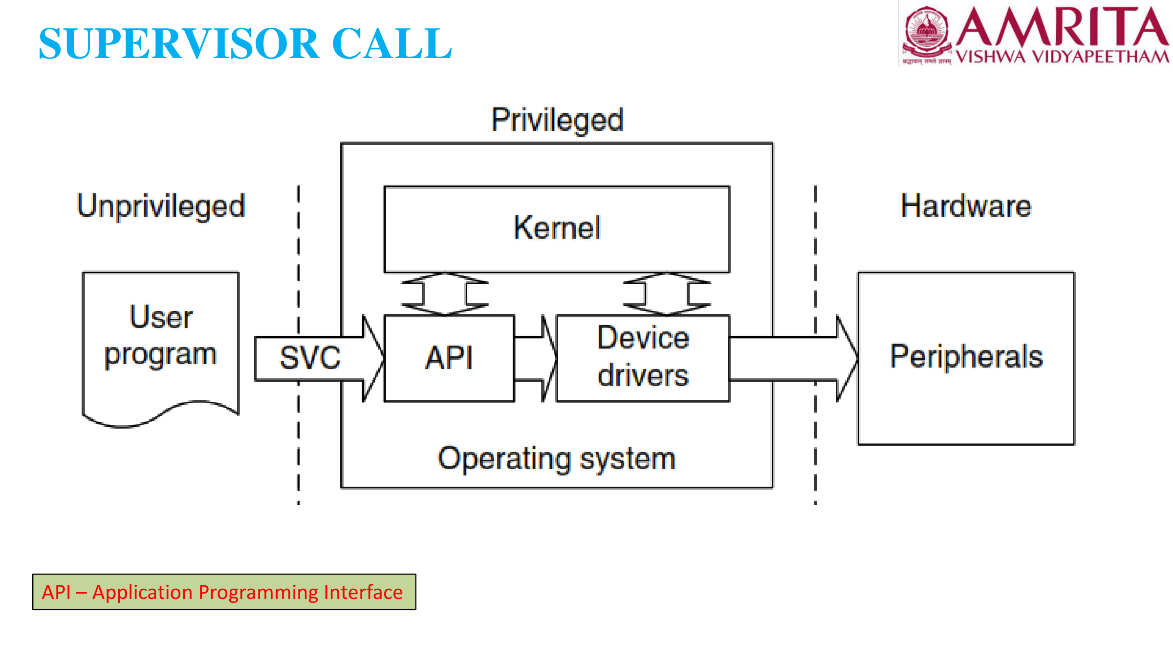
Mechanism of Parameter Passing:
- When the
SVCinstruction executes, hardware automatically pushes 8 registers onto the current stack: R0, R1, R2, R3, R12, LR, PC (return address), and xPSR. - Input arguments are passed in R0–R3 prior to executing
SVC. - The SVC Handler reads the stacked PC value, which points to the instruction immediately following
SVC. - The immediate 8-bit argument is extracted in software by inspecting the memory word preceding the stacked PC:
svc_number = ((uint8_t*)stacked_pc)[-2];
3. The Four Fault Exceptions & Status Registers
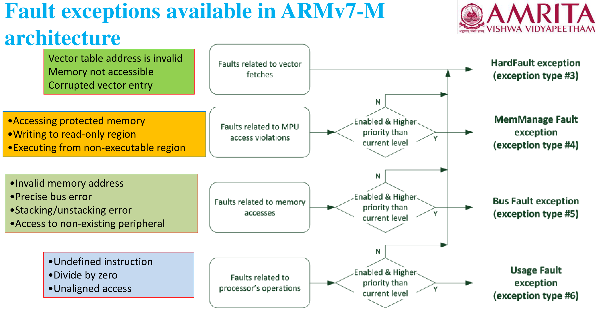
Summary of Fault Types:
- MemManage Fault (Exc #4): Memory Protection Unit (MPU) violation or accessing execute-never (XN) regions.
- Bus Fault (Exc #5): Memory system returns an error response (e.g., accessing non-existent memory address or invalid peripheral).
- Usage Fault (Exc #6): Execution errors (undefined instruction, division by zero, unaligned memory access, or trying to clear Thumb bit).
- HardFault (Exc #3): Generic, fixed-priority fault. Triggered when a fault cannot be handled by another handler or escalates.
Detailed Comparison of Fault Types:
| Fault Name | Exc # | Programmable Priority? | Exact Root Causes | Associated Status Registers |
|---|---|---|---|---|
| Memory Management Fault (MemManage) | 4 | Yes (via SHPR1) |
• MPU permission violation (unprivileged access to privileged memory). • Instruction fetch from Execute-Never ( XN) memory.• Stack access crossing MPU region boundaries. |
MMFSR (Memory Management Fault Status Register)MMFAR (Holds faulting address if MMARVALID is set) |
| Bus Fault | 5 | Yes (via SHPR1) |
• Bus error response on read/write transfers. • Precise Bus Fault: Processor knows exact faulting instruction and address. • Imprecise Bus Fault: Asynchronous error resulting from write buffers. • Stacking/unstacking memory bus errors. |
BFSR (Bus Fault Status Register)BFAR (Holds faulting address if BFARVALID is set) |
| Usage Fault | 6 | Yes (via SHPR1) |
• Undefined instruction execution. • Attempting to clear Thumb bit ( T=0 in EPSR) to switch to ARM state.• Unaligned memory access (if UNALIGN_TRP is set). • Divide by zero (if DIV_0_TRP is enabled). • Invalid EXC_RETURN value during exception return. |
UFSR (Usage Fault Status Register) |
| HardFault | 3 | No (Fixed at -1) | • Fault Escalation: Configurable fault occurs while its handler is disabled in SHCSR.• Fault occurring inside another fault handler with equal/higher priority. • Bus fault during vector table fetch. |
HFSR (Hard Fault Status Register) |
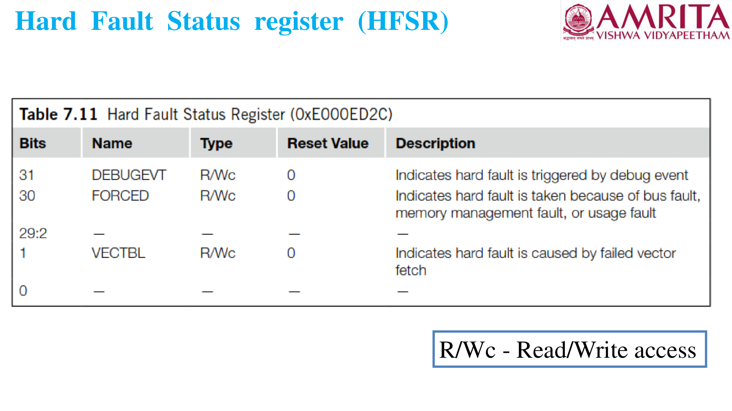
Critical Bits in HFSR:
- Bit 30 (FORCED): HardFault was triggered by escalation (e.g. a MemManage, Bus, or Usage fault occurred but was disabled).
- Bit 1 (VECTTBL): HardFault was triggered by a bus error during vector table read.
- Bit 31 (DEBUGEVT): HardFault resulted from a debug event when debug monitor was disabled.
Methods of Dealing with Faults (Ch 12 Slides 21–25):
- System Self-Reset: Initiated by setting the
SYSRESETREQbit in theAIRCRregister. Common in deeply embedded microcontrollers where state recovery is impossible. - Task Termination: In systems running an RTOS, the offending application task is killed by the OS kernel while the core and other tasks continue executing.
- Status Register Clearing: Fault status registers (CFSR, HFSR) retain status bits until cleared manually by writing
1to the respective bits (Write-1-to-Clear / R/W1C).
🔋 Unit II: Advanced Features & CoreSight Debug Architecture
Core Architecture1. CoreSight Debug Architecture (Ch 15 Slides 4–14)
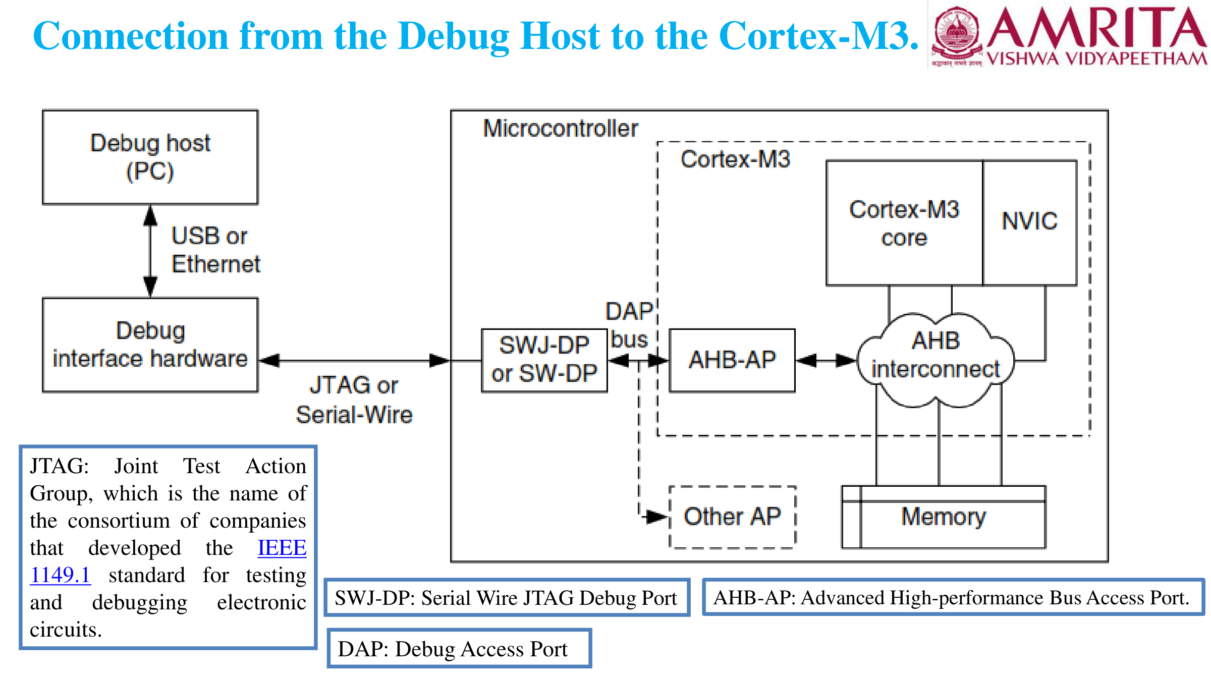
How to Draw and Label This Architecture in the Exam:
- Debug Host (PC): Runs Keil µVision / STM32CubeIDE. Sends debug packets over USB.
- Debug Interface Hardware (Probe): Hardware adapter (ST-Link / J-Link) that converts USB commands into JTAG (4-5 pins) or SWD (2 pins: SWCLK, SWDIO).
- SWJ-DP (Serial Wire JTAG Debug Port): The on-chip hardware interface supporting both JTAG and SWD protocols.
- DAP (Debug Access Port) Bus: Internal bus distributing debug commands from the debug port to multiple Access Ports.
- AHB-AP (Advanced High-Performance Bus Access Port): Bridges the debug port directly to the internal AHB system bus. Key Advantage: Allows the host PC to read and write memory, SRAM, and peripheral registers even while the CPU core is actively executing instructions!
- AHB Interconnect: Connects the Cortex-M3 core, NVIC, Flash, SRAM, and peripherals.
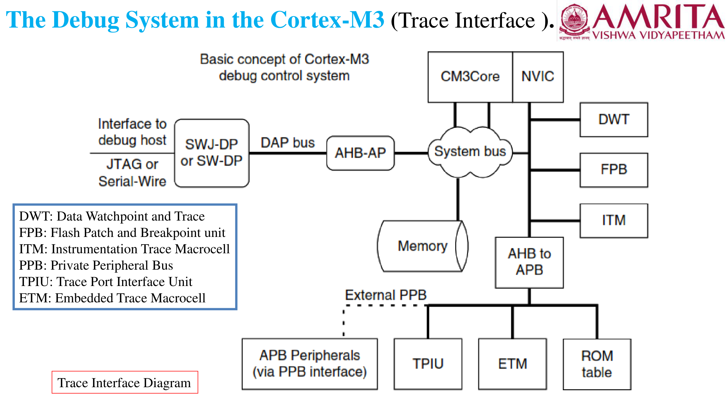
Functions of All 5 Trace & Debug Blocks:
- DWT (Data Watchpoint and Trace): Hardware unit that monitors memory addresses for read/write accesses, provides cycle counting, and event profiling.
- FPB (Flash Patch and Breakpoint): Hardware breakpoint comparator (typically 6 instruction breakpoints and 2 literal comparisons in Flash).
- ITM (Instrumentation Trace Macrocell): Software-driven trace unit. Allows code to output debug strings (like
printf) through the Serial Wire Output (SWO) pin without stopping the core. - ETM (Embedded Trace Macrocell): Real-time instruction trace capturing complete instruction flow. Outputs data via the high-speed Trace Port Interface Unit (TPIU).
- TPIU (Trace Port Interface Unit): Formats and streams trace data packets out of the microcontroller to external hardware trace analyzers.
Comparison of Debug Modes (Ch 15 Slides 15 & 16):
| Feature | Halt Mode | Debug Monitor Mode |
|---|---|---|
| CPU Execution | Completely stopped (CPU halted). | CPU continues running; enters Exception 12 (Debug Monitor ISR). |
| SysTick Timer | Stopped while CPU is halted. | SysTick counter continues running normally. |
| Interrupt Handling | Interrupts are pended and masked during stepping. | Higher-priority interrupts can still preempt the debug monitor. |
| Typical Use Case | Initial firmware development, single-stepping bare-metal code. | Time-critical applications (motor control, power electronics) where stopping the clock causes hardware damage. |
2. SysTick Timer (Ch 14 Slides 1–5)
SYST_RVR, counts down to 0, sets COUNTFLAG (bit 16 in SYST_CSR), and generates Exception 15 (SysTick).
The 4 SysTick Registers:
| Register Name | Address Offset | Bit Fields & Functionality |
|---|---|---|
SYST_CSR |
0xE000E010 | Control & Status Register: • Bit 0 ( ENABLE): 1 = Counter running, 0 = Disabled.• Bit 1 ( TICKINT): 1 = Generates SysTick exception when counter reaches 0.• Bit 2 ( CLKSOURCE): 0 = External reference clock, 1 = Core clock.• Bit 16 ( COUNTFLAG): Set to 1 when counter counts from 1 to 0; cleared by reading CSR. |
SYST_RVR |
0xE000E014 | Reload Value Register: Bits [23:0] hold the 24-bit value loaded into CVR upon reaching 0. Example: Reload = 999 produces a tick every 1000 clock cycles. |
SYST_CVR |
0xE000E018 | Current Value Register: Bits [23:0] hold the live counter value. Writing any value to CVR clears it to 0 and clears COUNTFLAG. |
SYST_CALIB |
0xE000E01C | Calibration Value Register: Factory calibration for 10ms tick rate. |
3. Sleep-on-Exit & Wake-up Interrupt Controller (WIC)
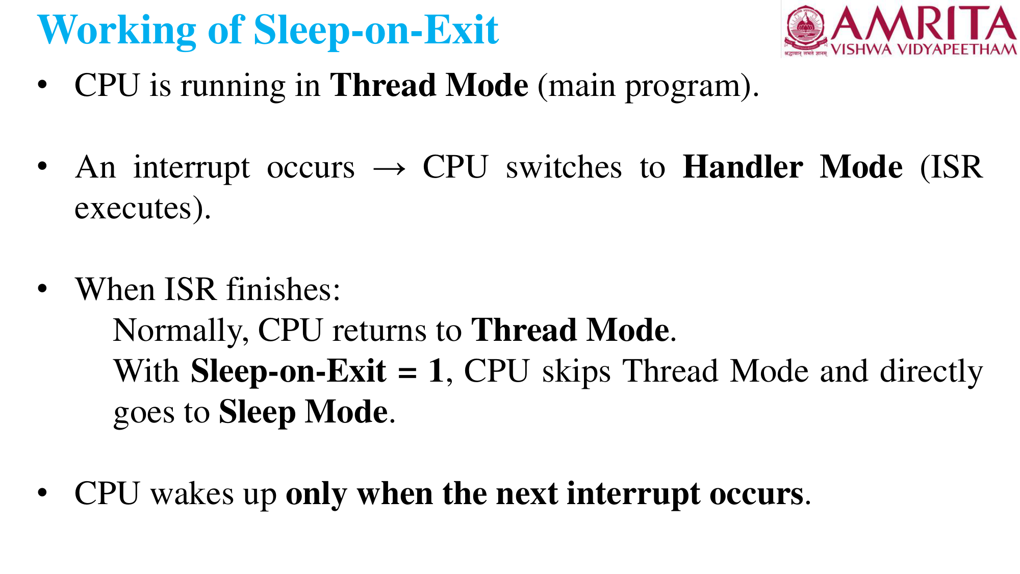
Working of Sleep-on-Exit:
- Enabled by setting the
SLEEPONEXITbit in the System Control Register (SCR). - Normal Operation: CPU runs in Thread mode $\rightarrow$ Interrupt occurs $\rightarrow$ Enters ISR $\rightarrow$ Exits ISR $\rightarrow$ Unstacks registers and returns to Thread mode.
- With Sleep-on-Exit: When the last active ISR finishes, instead of popping the stack and waking up Thread mode, the CPU immediately returns to Sleep mode.
- Advantage: Eliminates the energy and clock cycle overhead of stack restoration in battery-powered, interrupt-driven sensor nodes.
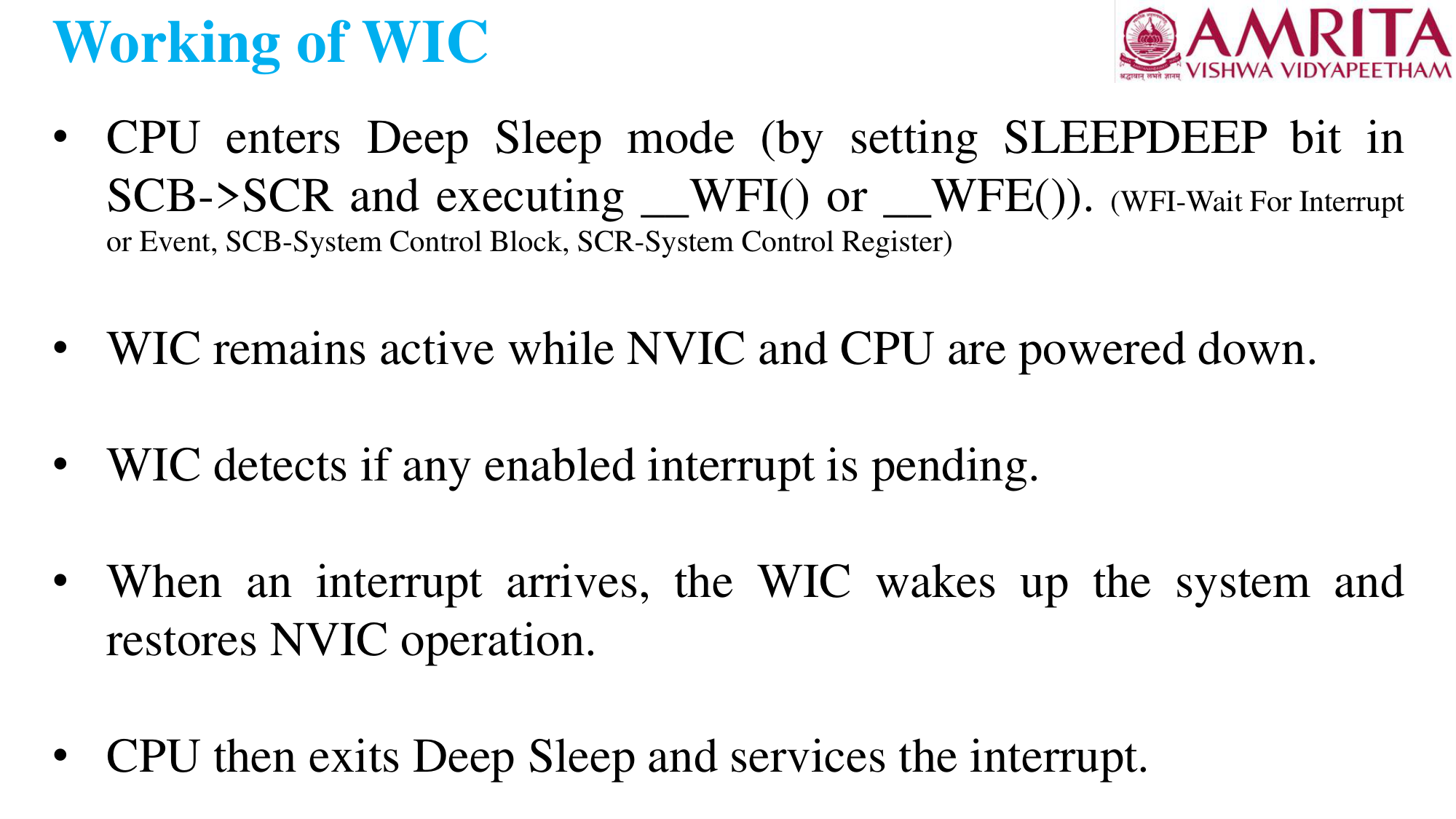
Need and Operation of WIC:
- The Problem in Deep Sleep: To minimize power consumption, the microcontroller enters Deep Sleep (
SLEEPDEEPbit set in SCR). The main oscillator, processor core clock, and NVIC clocks are completely shut down. The NVIC cannot detect interrupts! - The Solution (WIC): The Wake-up Interrupt Controller is a separate, ultra-low-power hardware block operating in the always-on power domain.
- Working: When an external pin goes active, the WIC detects the signal and pulses the Power Management Unit (PMU). The PMU restarts the main oscillators, powers up the core and NVIC, and hands off the interrupt request to the NVIC for execution.
4. Multiprocessor Communication & Self-Reset Control
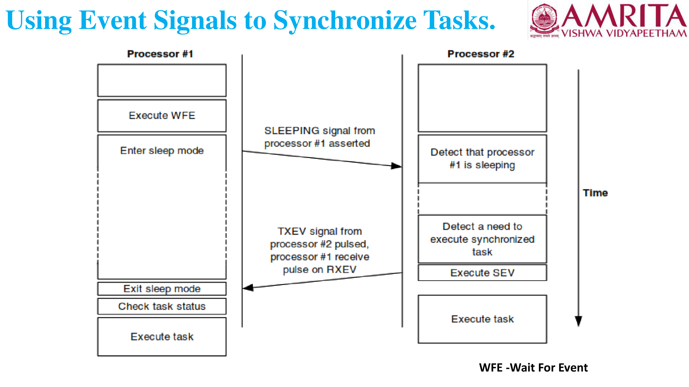
Instructions & Hardware Signals:
SEV(Send Event): Instruction executed by a core to pulse itsTXEVoutput pin to notify peer processors or peripherals.WFE(Wait For Event): Instruction that places the core into low-power idle until an event signal arrives at itsRXEVinput or an interrupt occurs.
Self-Reset Control (Ch 14 Slide 18 & 19):
The Cortex-M3 provides two self-reset control features via the Application Interrupt and Reset Control Register (AIRCR) located at address 0xE000ED0C. To write to AIRCR, a security key (0x05FA) must be written to bits [31:16]:
SYSRESETREQ(Bit 2): Requests a system-level reset. Pulls the microcontroller\'s reset line, resetting the core, memories, and all external peripherals (GPIO, Timers, UART).VECTRESET(Bit 0): Resets only the Cortex-M processor core. It does not reset peripherals outside the core. Targeted strictly for debugger use.
🏛️ Unit I: Cortex-M3 Architecture, Registers & Operating Modes
Foundational Theory1. Core Architecture & Operating Modes (Ch 4 Slides 6–28)
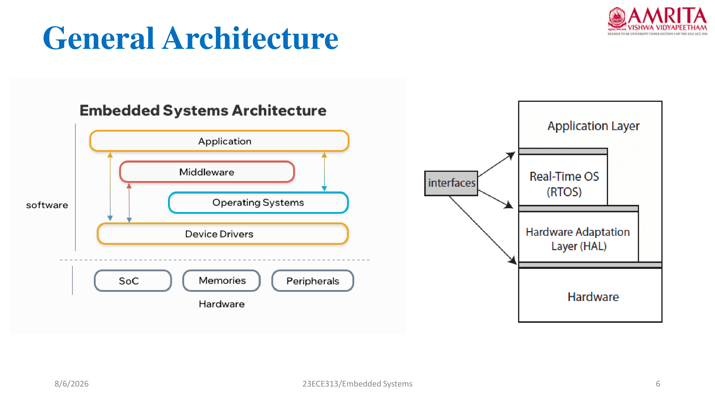
Architectural Blocks:
- Processor Core: Central processing unit containing 32-bit ALU, 3-stage pipeline, and register bank.
- NVIC (Nested Vectored Interrupt Controller): Handles up to 240 external interrupt inputs with priority management.
- Bus Interfaces: Connects internal core to Code memory, SRAM, and Peripherals via AHB/APB interconnect.
- Debug Support: CoreSight debugging system with SWJ-DP, AHB-AP, and trace blocks.
Operating States, Modes, and Privilege Levels (Ch 4 Slides 26–28):
| Classification | State / Mode / Level | Description & Rules |
|---|---|---|
| Operating States | Thumb State | Cortex-M3 runs exclusively in Thumb state (Thumb-2 instruction set mixing 16-bit and 32-bit instructions). It does not support the classic 32-bit ARM state. Bit 0 of instruction addresses must always be 1. |
| Operating States | Debug State | Entered when processor is halted by a debugger. |
| Operating Modes | Thread Mode | The default mode for user applications and background software. Can be either Privileged or Unprivileged. |
| Operating Modes | Handler Mode | Entered automatically when executing an exception handler or ISR. Always Privileged. |
| Privilege Levels | Privileged Level | Full access to all memory regions, system control space, and instructions (e.g. MSR, CPSID). |
| Privilege Levels | Unprivileged Level | Restricted access. Limited access to MPU-protected regions; cannot access NVIC or System Control Space. Cannot switch back to Privileged mode directly (must execute SVC). |
2. Cortex-M3 Register Bank (Ch 4 Slides 29–48)
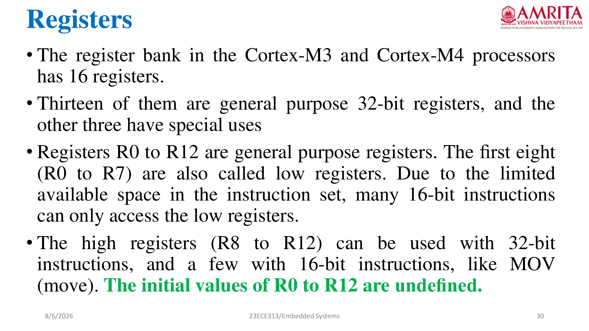
Detailed Breakdown of Every Register:
- R0 – R12 (General Purpose Registers): 32-bit registers for data processing. R0–R7 are low registers (accessible by all 16-bit Thumb instructions); R8–R12 are high registers.
- R13 (SP - Stack Pointer): Physically banked into two separate 32-bit stack pointers:
- MSP (Main Stack Pointer): Default at reset. Used by operating system kernel, main system code, and all exception handlers.
- PSP (Process Stack Pointer): Used exclusively by application tasks in Thread Mode to isolate user stack from kernel stack.
- Lowest 2 bits of both SPs are always 0 (4-byte / word alignment).
- R14 (LR - Link Register): Stores the return address for function calls. During exception entry, the LR is automatically updated with a special
EXC_RETURNvalue. - R15 (PC - Program Counter): Points to the current instruction address + 4 (due to pipeline prefetch). Bit 0 must always be 1 (Thumb indicator).
Special Registers: xPSR, Mask Registers & CONTROL (Ch 4 Slides 39–48):
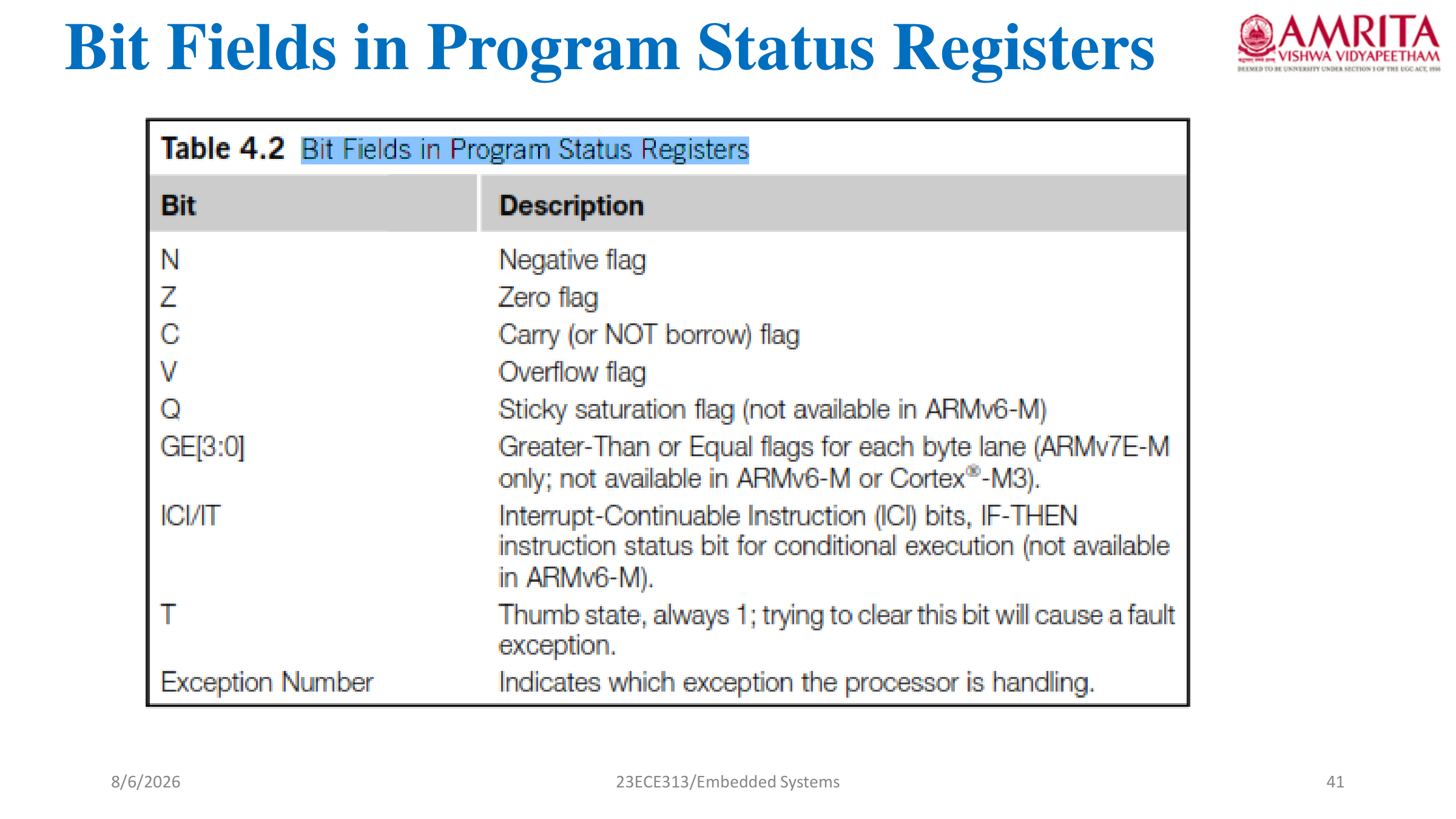
The Three Program Status Registers:
- APSR (Application PSR): Holds condition flags: N (Negative, bit 31), Z (Zero, bit 30), C (Carry, bit 29), V (Overflow, bit 28), and Q (Saturation flag, bit 27). The Q flag is sticky.
- IPSR (Interrupt PSR): Bits [8:0] hold the currently executing Exception Number (e.g., 0 = Thread mode, 15 = SysTick, 16+ = External IRQs).
- EPSR (Execution PSR):
- Bit 24 (T - Thumb bit): Must always be
1. Clearing it triggers a Usage Fault! - Bits [15:10, 26:25] (ICI/IT): Interruptible-Continuable Instruction (ICI) bits save intermediate transfer counts during multi-cycle instructions (
LDM/STM) so interrupted instructions can resume where they left off; If-Then (IT) bits hold conditional execution states for the IT block.
- Bit 24 (T - Thumb bit): Must always be
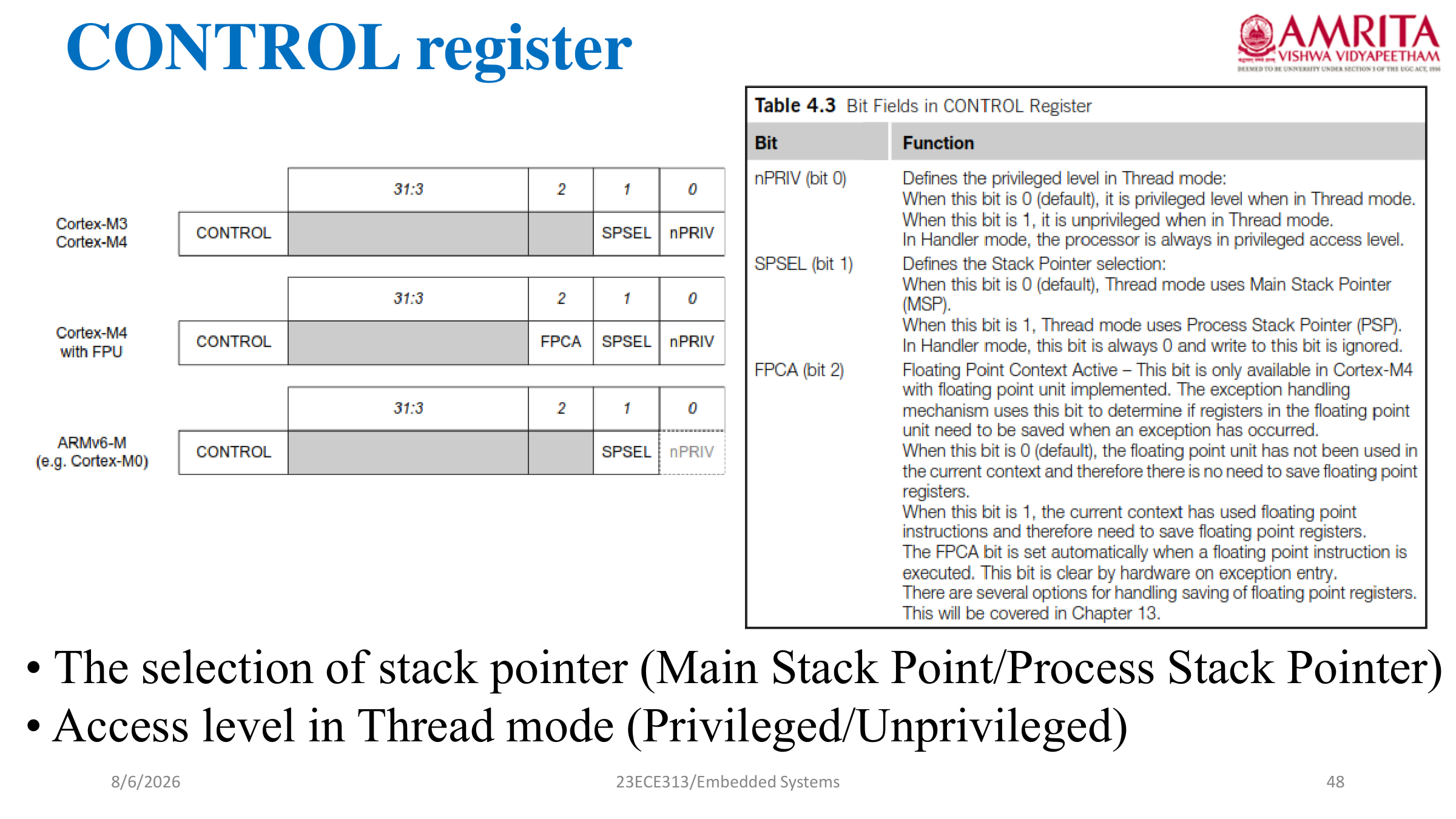
The 2 Bits of the CONTROL Register:
- Bit 0 (
nPRIV): Defines thread mode privilege level:0= Privileged thread mode.1= Unprivileged thread mode.
- Bit 1 (
SPSEL): Selects active stack pointer in Thread mode:0= Main Stack Pointer (MSP) active.1= Process Stack Pointer (PSP) active.
- In Handler mode, MSP is always used; SPSEL cannot be changed!
Interrupt Mask Registers (PRIMASK, FAULTMASK, BASEPRI):
- PRIMASK (1 bit): When set to 1, disables all configurable exceptions/interrupts. Only NMI and HardFault can still preempt. Modified via
CPSID i/CPSIE i. - FAULTMASK (1 bit): When set to 1, disables all exceptions except NMI (HardFault is also disabled). Effective priority becomes -1. Modified via
CPSID f/CPSIE f. - BASEPRI (8 bits): Disables all interrupts with priority level equal to or lower than the programmed threshold value. Unaffected interrupts with higher priority can still preempt.
3. 3-Stage Pipeline (Ch_Txt1 Slides 14 & 15)
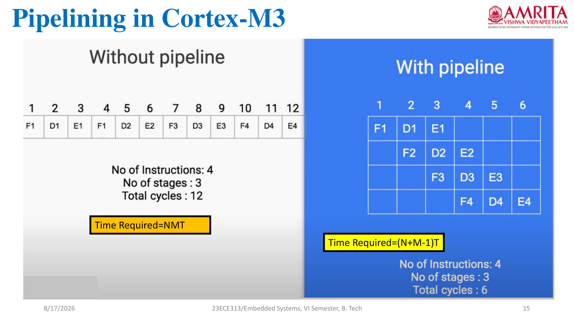
Pipeline Stages:
- Stage 1 (Fetch): Fetches instruction from instruction memory (Flash).
- Stage 2 (Decode): Decodes opcode and registers.
- Stage 3 (Execute): ALU executes instruction, writes results back to registers or loads/stores data.
- Throughput: Takes 3 clock cycles to execute a single instruction from start to finish (latency = 3), but because operations overlap, effective throughput is 1 instruction per cycle under sequential program execution.
- Branch Speculation: When a conditional branch occurs, pipeline flushing causes a 2-cycle penalty.
4. Bus Interfaces (Ch_Txt1 Slides 16 & 17)
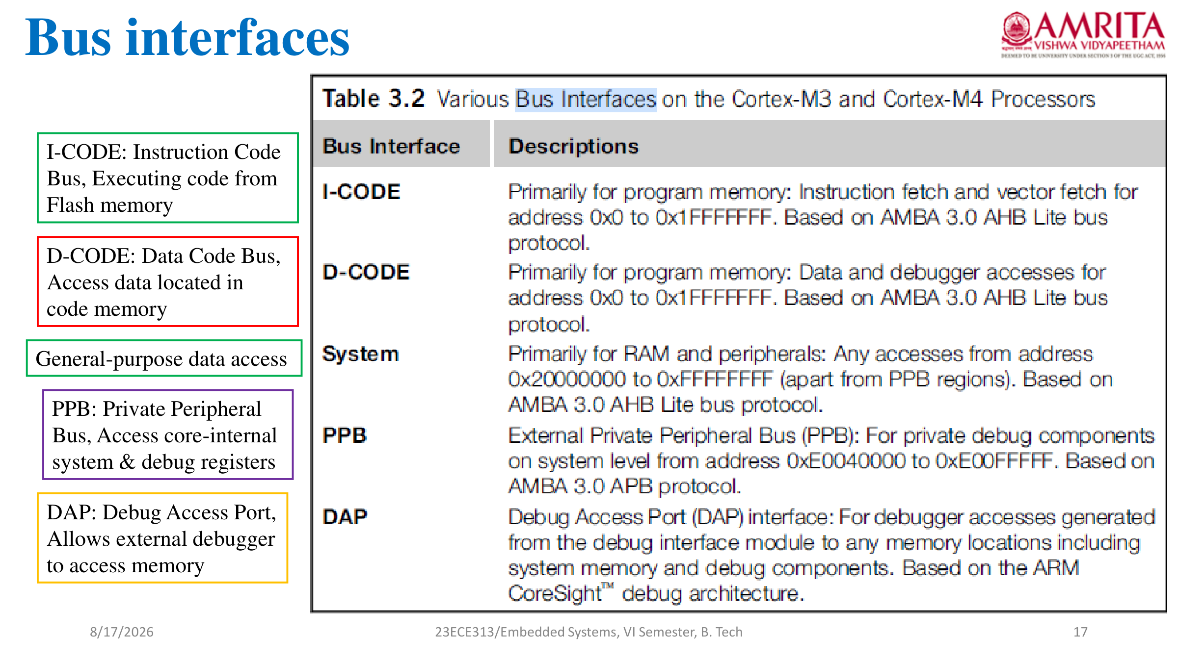
Bus Definitions:
- I-Code Bus: Advanced High-performance Bus (AHB-Lite) used for instruction fetches from Code memory (
0x00000000 - 0x1FFFFFFF). - D-Code Bus: AHB-Lite bus used for data accesses and literal lookups from Code memory.
- System Bus: Connects core to SRAM, external memories, and system peripherals (
0x20000000 - 0xDFFFFFFF). - Private Peripheral Bus (PPB): Connects core to internal private peripherals (NVIC, SysTick, MPU, DWT, FPB, ITM) in the memory space
0xE0000000 - 0xE00FFFFF.
🗺️ Unit I: Memory Map, Bit-Banding, Reset Sequence & NVIC
High Probability Exam Topics1. 4GB Linear Memory Map & Attributes (Ch 4 Slides 49–54, Ch_Txt1 Slides 11–13)
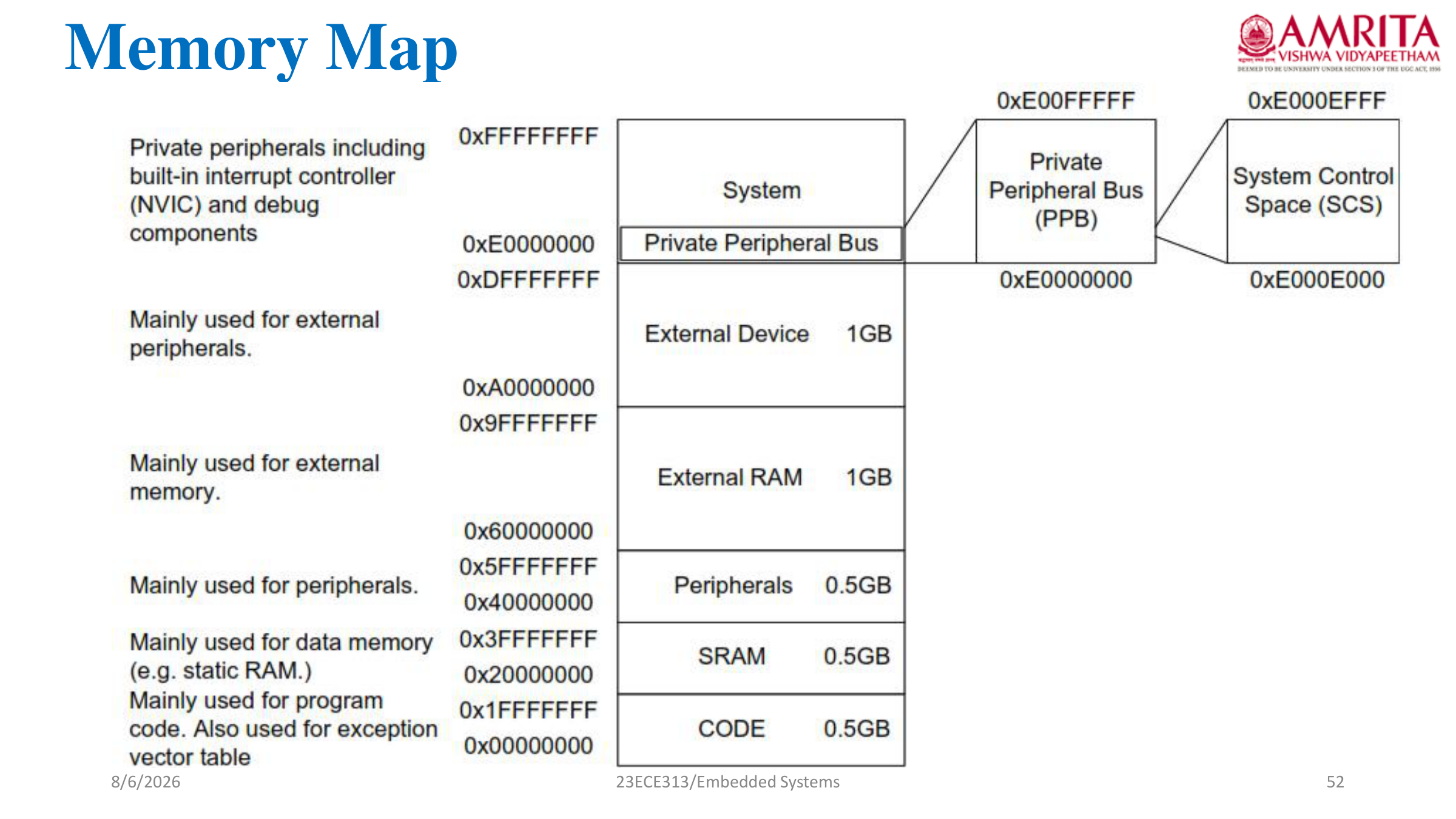
Memory Regions:
- Code (0.5 GB:
0x00000000 - 0x1FFFFFFF): Contains Vector Table, Flash ROM, and boot code. Executed via I-Code bus. - SRAM (0.5 GB:
0x20000000 - 0x3FFFFFFF): Internal RAM for data, stack, and heap. First 1 MB contains SRAM Bit-band region. - Peripheral (0.5 GB:
0x40000000 - 0x5FFFFFFF): Internal on-chip peripherals (GPIO, Timers, ADC, UART). First 1 MB contains Peripheral Bit-band region. Execute-Never (XN). - External RAM (1.0 GB:
0x60000000 - 0x9FFFFFFF): Off-chip SRAM, SDRAM, or NOR Flash. - External Device (1.0 GB:
0xA0000000 - 0xDFFFFFFF): Off-chip memory-mapped I/O devices. Non-bufferable, non-cacheable,XN. - System / Private Peripheral Bus (0.5 GB:
0xE0000000 - 0xFFFFFFFF): PPB memory space containing NVIC, SysTick, MPU, and CoreSight debug registers.
Memory Access Attributes (Ch_Txt1 Slides 11–13):
- Bufferable: Memory write transfers can be handled by a write buffer while the processor continues executing subsequent instructions without stalling.
- Cacheable: Memory reads can be copied into high-speed local cache memories.
- Executable (XN): Execute-Never attribute. Attempting to fetch instructions from an XN region (such as Peripherals or System Space) triggers an immediate MemManage Fault.
- Shareable: Data memory accessible by multiple bus masters (e.g., DMA and CPU). Memory system enforces hardware cache coherency.
2. Bit-Banding: Architecture, Advantages & Calculations (Ch_Txt1 Slides 2–10)
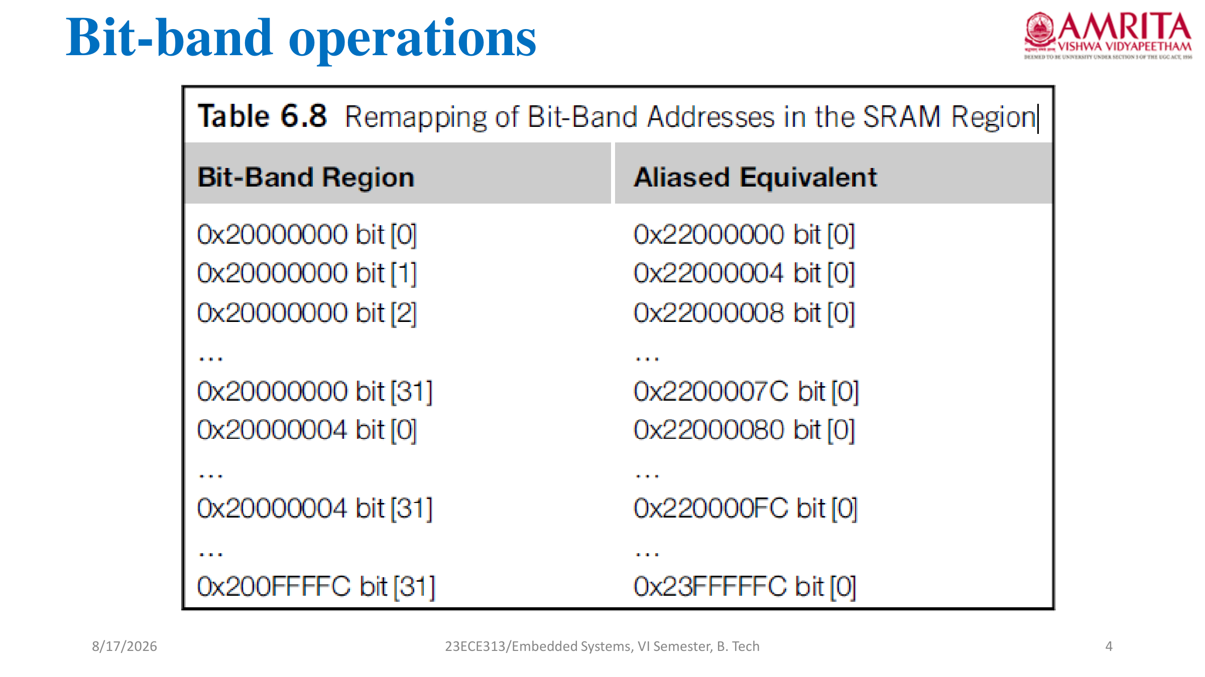
The Two Bit-Band Regions in Cortex-M3:
- SRAM Bit-Band Region:
0x20000000 - 0x200FFFFF(1 MB) $\longrightarrow$ Maps to Alias:0x22000000 - 0x23FFFFFF(32 MB). - Peripheral Bit-Band Region:
0x40000000 - 0x400FFFFF(1 MB) $\longrightarrow$ Maps to Alias:0x42000000 - 0x43FFFFFF(32 MB). - Expansion Ratio: Every single 1-bit in the target region expands into a full 32-bit word (4 bytes) in the alias region ($1\text{ MB} \times 32 = 32\text{ MB}$).
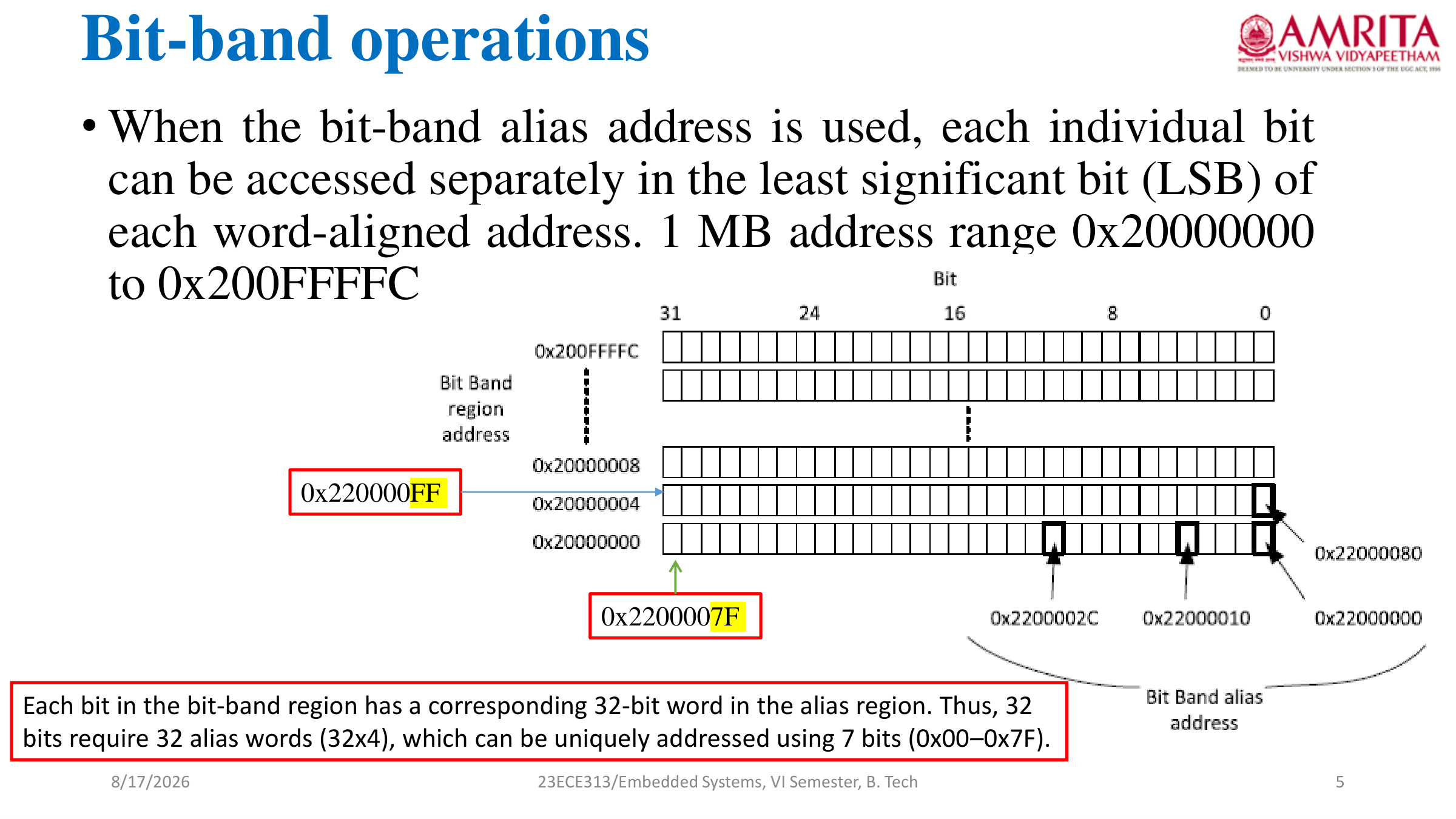
Advantages of Bit-Banding:
- Atomic Bit Manipulation: Eliminates race conditions in multi-threaded/RTOS environments. A task can set or clear a flag bit without disabling interrupts!
- Code Density & Execution Speed: A bit manipulation requires only a single
STRinstruction instead ofLDR$\rightarrow$ORR/AND$\rightarrow$STR(reduces 3 instructions to 1). - Simplified I/O Toggling: Directly toggles GPIO pins or serial communication lines (I2C/SPI bit-banging) with atomic writes.
Bit-Band Alias Address Calculation Formula & Numerical:
In hexadecimal notation: Multiply offset by
0x20 (decimal 32) and bit number by 0x4.
"Manipulate bit $x = 20$ of a 32-bit register located at address $y = 0\text{x}40020014$. Calculate the alias address (Peripheral Alias Base = $0\text{x}42000000$, Peripheral Bit-Band Base = $0\text{x}40000000$)."
Step-by-Step Solution:
1. Byte Offset = $y - \text{Bit-band Base} = 0\text{x}40020014 - 0\text{x}40000000 = 0\text{x}20014$.
2. Multiply Byte Offset by 32 ($0\text{x}20$ in hex):
$$0\text{x}20014 \times 0\text{x}20 = 0\text{x}400280$$
3. Multiply Bit Number ($x = 20 = 0\text{x}14$) by 4:
$$20 \times 4 = 80 = 0\text{x}50$$
4. Calculate Alias Address:
$$\text{Alias Address} = 0\text{x}42000000 + 0\text{x}400280 + 0\text{x}50 = \mathbf{0x424002D0}$$
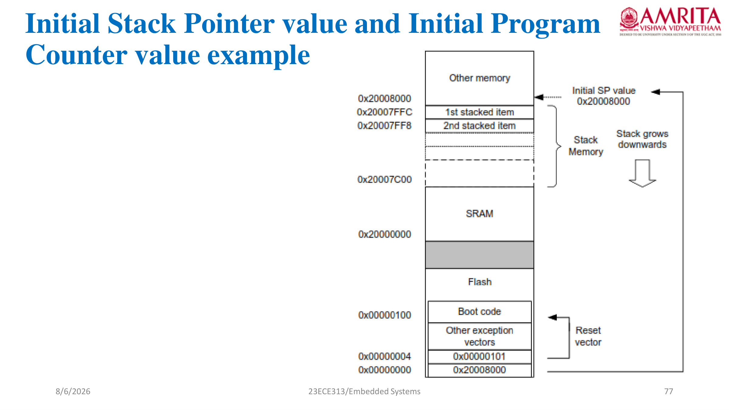
3. Reset Sequence & Vector Table Architecture (Ch 4 Slides 75–77)
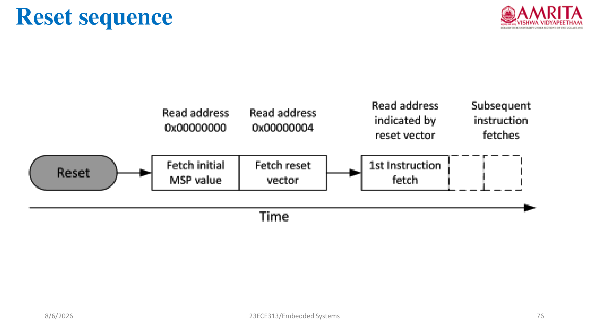
Hardware Reset Execution Steps:
- Step 1: System reset signal is de-asserted; clock stabilizes.
- Step 2 (Fetch Vector 0): Hardware fetches the 32-bit word from memory address
0x00000000and loads it directly into the Main Stack Pointer (MSP). This ensures a valid stack exists before executing any code! - Step 3 (Fetch Vector 1): Hardware fetches the 32-bit word from memory address
0x00000004and loads it directly into the Program Counter (PC). This word contains the address of theReset_Handlerfunction. Bit 0 of this address must be1to specify Thumb state. - Step 4: Processor begins instruction execution at
Reset_Handlerin Privileged Thread Mode.
4. NVIC: Preempt Priority, Sub-Priority & Pending Behavior (Ch_Txt1)
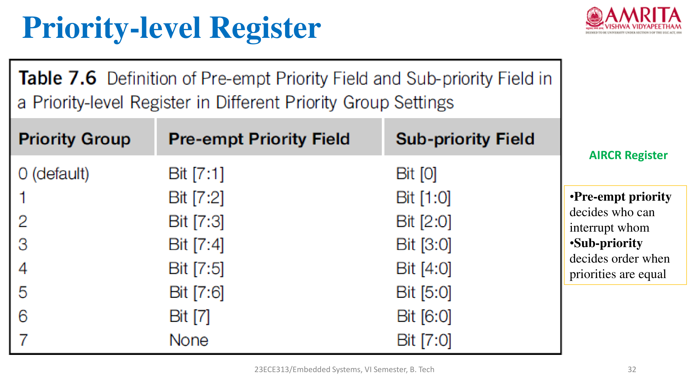
Priority Rules:
- Each interrupt priority level register holds an 8-bit priority value (microcontrollers implement top 3 to 8 bits). Smaller numerical values indicate higher logical priority (0 is highest).
- The
PRIGROUPfield in the Application Interrupt and Reset Control Register (AIRCR) splits the priority bits into two fields:- Preemption Priority: Determines whether an arriving interrupt can interrupt (nest inside) an currently executing ISR.
- Sub-Priority: When two pending interrupts have the identical preemption priority, the one with the smaller sub-priority value executes first. Sub-priority does NOT cause preemption!
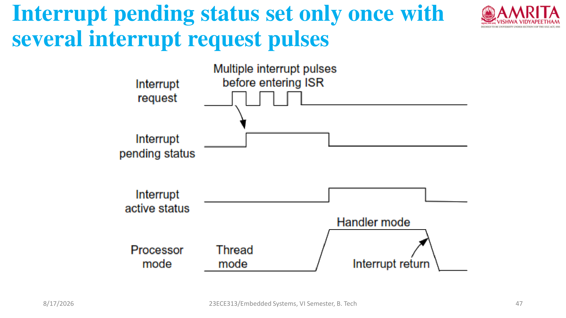
Pending Behavior:
- The NVIC is designed to accept both pulsed and level interrupt inputs.
- If multiple pulses occur on an interrupt line while the interrupt is pending or currently executing, the NVIC records the pending status only once.
- Software can read/set/clear pending status via the NVIC Interrupt Set-Pending Registers (
NVIC_ISPR) and Interrupt Clear-Pending Registers (NVIC_ICPR).
💻 Coding Mastery: STM32F446RE Register-Level Programs (15–20 Marks)
Critical Exam SectionEvery program here is written directly for the STM32F446RE using bare-metal register manipulation (CMSIS syntax). Each code section includes a step-by-step logic explanation, a complete register breakdown table, and an execution flow diagram.
1. GPIO: Push Button Toggle LED with Software Debouncing (Lab Exp 1)
• PA5: Connected to on-board Green LED (LD2). High = ON, Low = OFF.
• PC13: Connected to on-board Blue Push Button (B1). Connected with external pull-up. Reads
1 when released, 0 when pressed (Active-LOW).
Register Breakdown for GPIO Program:
| Register Name | Full Name & Purpose | Exact Bits Used & Meaning |
|---|---|---|
RCC->AHB1ENR |
AHB1 Peripheral Clock Enable Register | • Bit 0 (GPIOAEN): Set to 1 to supply clock to Port A.• Bit 2 (GPIOCEN): Set to 1 to supply clock to Port C. Without this, GPIO registers do not respond! |
GPIOA->MODER |
GPIO Port Mode Register (Port A) | Each pin uses 2 bits. For PA5: Bits [11:10]. • 00 = Input• 01 = General Purpose Output (Written as 1U << (5*2))• 10 = Alternate Function• 11 = Analog |
GPIOC->MODER |
GPIO Port Mode Register (Port C) | For PC13: Bits [27:26]. Cleared to 00 for Input mode. |
GPIOC->IDR |
GPIO Port Input Data Register | Read-only register. Bit 13 reflects the digital voltage level at PC13 pin. (GPIOC->IDR & (1U << 13)) isolates pin 13. |
GPIOA->ODR |
GPIO Port Output Data Register | Read/Write register. Bit 5 controls PA5 voltage level. GPIOA->ODR ^= (1U << 5); flips bit 5 between 0 and 1, toggling the LED. |
Complete Source Code:
#include "stm32f4xx.h"

// Software delay function for contact debouncing
void delay_ms(uint32_t ms) {
    uint32_t count = (SystemCoreClock / 10000) * ms;
    for (volatile uint32_t i = 0; i < count; i++) {
        __NOP();
    }
}

int main(void) {
    // 1. Enable AHB1 bus clocks for GPIO Port A and Port C
    RCC->AHB1ENR |= RCC_AHB1ENR_GPIOAEN | RCC_AHB1ENR_GPIOCEN;

    // 2. Configure PA5 (LED) as General Purpose Output (Mode '01')
    GPIOA->MODER &= ~(3U << (5 * 2)); // Clear bits [11:10]
    GPIOA->MODER |=  (1U << (5 * 2)); // Set to 01 (Output)

    // 3. Configure PC13 (Button) as Input Mode (Mode '00')
    GPIOC->MODER &= ~(3U << (13 * 2)); // Clear bits [27:26] to 00

    uint8_t last_button_state = 1; // Default state: released (Active-LOW)

    while (1) {
        // Read current state of Pin 13 from IDR
        uint8_t current_state = (GPIOC->IDR & (1U << 13)) ? 1 : 0;

        // Detect Falling Edge: transition from Released (1) to Pressed (0)
        if (last_button_state == 1 && current_state == 0) {
            GPIOA->ODR ^= (1U << 5); // Toggle LED via ODR bit 5
            delay_ms(50);             // 50ms software debounce
        }
        last_button_state = current_state;
    }
}
2. Timers: Accurate Delay Generation using 32-bit Timer 5 (Lab Exp 2)
STM32F446RE default internal RC oscillator (HSI) runs at $f_{sys} = 16\text{ MHz}$.
Timer Clock Frequency = \frac{f_{sys}}{PSC + 1} = \frac{16\text{ MHz}}{15999 + 1} = 1000\text{ Hz} = 1\text{ kHz}
Since the timer counts at $1000\text{ Hz}$, each tick is exactly $1\text{ ms}$.
\text{For a delay of } t \text{ seconds: } ARR = (t \times 1000) - 1
Register Breakdown for Timer Program:
| Register Name | Full Name & Purpose | Exact Bits Used & Meaning |
|---|---|---|
RCC->APB1ENR |
APB1 Peripheral Clock Enable Register | • Bit 3 (TIM5EN): Enables clock for Timer 5 on the APB1 peripheral bus. |
TIM5->PSC |
Timer 5 Prescaler Register (16-bit) | Divides the incoming bus clock. Value loaded is 15999 ($16000 - 1$). Frequency becomes $16\text{ MHz}/16000 = 1\text{ kHz}$. |
TIM5->ARR |
Timer 5 Auto-Reload Register (32-bit) | Defines the ceiling of the counter in up-counting mode. When CNT reaches ARR, the counter overflows to 0 and asserts the Update Interrupt Flag (UIF). |
TIM5->CNT |
Timer 5 Counter Register (32-bit) | Holds the current count value. Cleared to 0 prior to starting. |
TIM5->CR1 |
Timer 5 Control Register 1 | • Bit 0 (CEN - Counter Enable): 1 starts counting; 0 stops the counter. |
TIM5->SR |
Timer 5 Status Register | • Bit 0 (UIF - Update Interrupt Flag): Set to 1 by hardware upon counter overflow/reload. Cleared by writing 0 by software. |
Complete Source Code:
#include "stm32f4xx.h"

void delay_seconds(uint32_t seconds) {
    // 1. Enable TIM5 peripheral clock on APB1 bus (Bit 3)
    RCC->APB1ENR |= RCC_APB1ENR_TIM5EN;

    // 2. Configure Timer Prescaler (PSC) for 1 ms tick resolution
    // Counter Clock = 16 MHz / (15999 + 1) = 1000 Hz = 1 ms per count
    TIM5->PSC = 15999;

    // 3. Set Auto-Reload Register (ARR) for requested seconds
    TIM5->ARR = (seconds * 1000) - 1;

    // 4. Reset counter register to 0
    TIM5->CNT = 0;

    // 5. Start the timer by setting Counter Enable (CEN) bit in CR1
    TIM5->CR1 |= TIM_CR1_CEN;

    // 6. Wait until Update Interrupt Flag (UIF) in Status Register is set
    while (!(TIM5->SR & TIM_SR_UIF)) {
        __NOP(); // Wait for counter overflow
    }

    // 7. Clean up: clear UIF flag and stop timer counter
    TIM5->SR  &= ~TIM_SR_UIF;
    TIM5->CR1 &= ~TIM_CR1_CEN;
}
3. PWM Generation using Timer 2 Channel 1 on PA5 (Lecture Slides)
• System Clock $f_{sys} = 16\text{ MHz}$. Target PWM Frequency $f_{PWM} = 1\text{ kHz}$.
f_{PWM} = \frac{f_{sys}}{(PSC + 1)(ARR + 1)} \implies 1000 = \frac{16\times 10^6}{(0 + 1)(ARR + 1)} \implies ARR = 15999
• Target Duty Cycle $D = 40\%$:
\text{Duty Cycle} = \frac{CCR1}{ARR + 1} \times 100\% \implies CCR1 = 0.40 \times 16000 = 6400
• Output Pin: PA5 mapped to
AF1 (Timer 2 Channel 1).
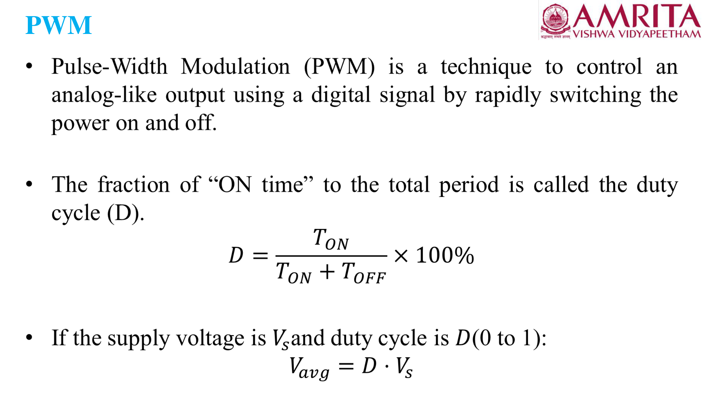
How to Explain This Diagram in the Exam:
- Definition: Pulse Width Modulation (PWM) is a technique used to generate analog-like average voltage levels using a digital signal by rapidly toggling power ON and OFF at a fixed frequency.
- Duty Cycle Formula: $D = \frac{T_{on}}{T_{on} + T_{off}} \times 100\% = \frac{T_{on}}{T_{period}} \times 100\%$.
- Average Output Voltage: $V_{avg} = D \times V_{supply}$. For $V_{supply} = 5\text{ V}$ and $D = 40\%$, $V_{avg} = 0.40 \times 5 = 2.0\text{ V}$.
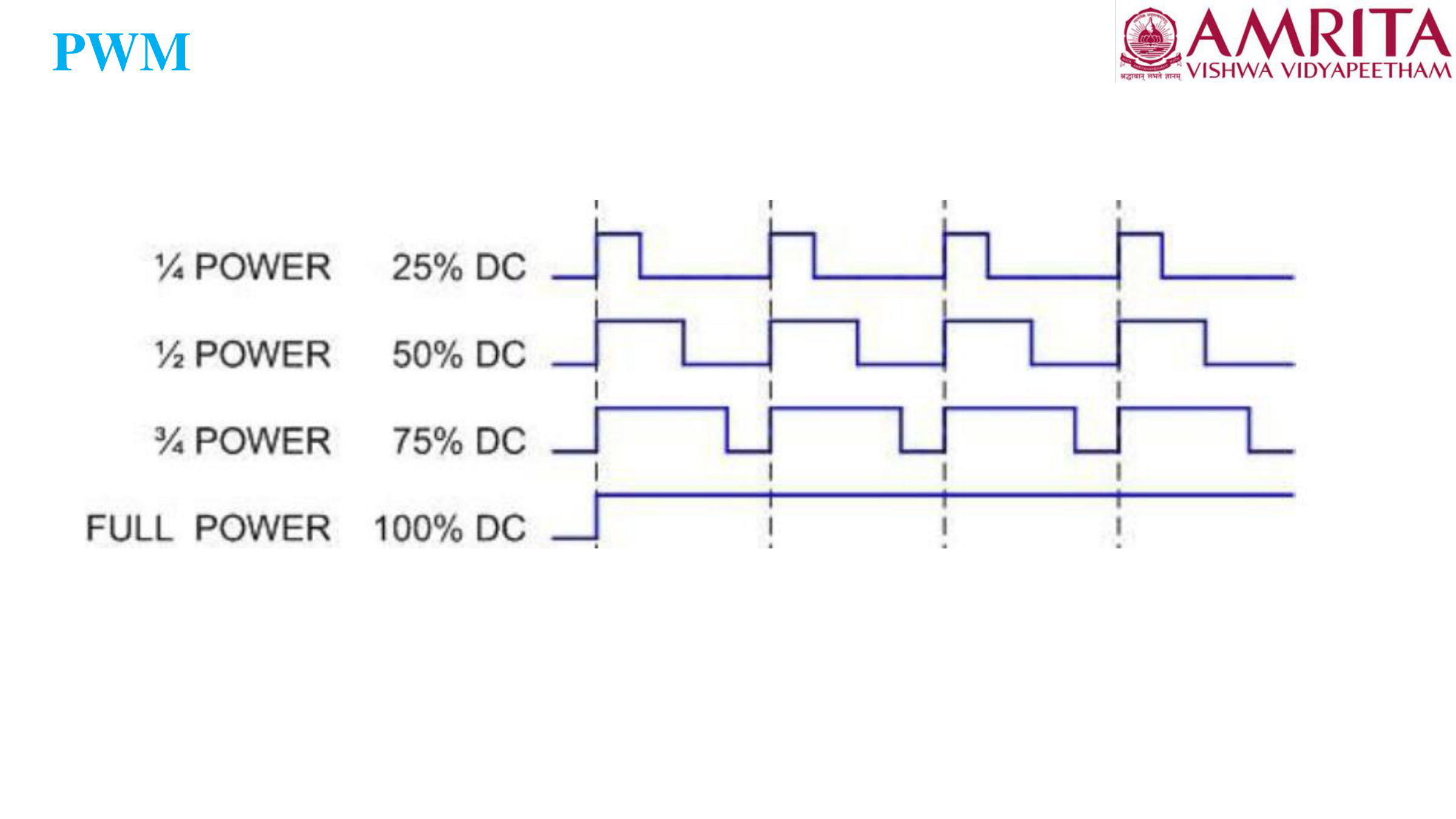
Waveform Analysis:
- 25% Duty Cycle: $T_{on} = 0.25 \times T$. Transmits 25% of maximum electrical power.
- 50% Duty Cycle: Symmetrical square wave ($T_{on} = T_{off}$). Transmits 50% power ($V_{avg} = 0.5 V_{cc}$).
- 75% Duty Cycle: High for three-quarters of period. Transmits 75% power.
- 100% Duty Cycle: Continuous DC high ($T_{on} = T$, $T_{off} = 0$). Maximum power output.
Register Breakdown for PWM Program:
| Register Name | Full Name & Purpose | Exact Bits Used & Meaning |
|---|---|---|
GPIOA->AFR[0] |
GPIO Alternate Function Low Register | Controls alternate functions for pins PA0 to PA7 (4 bits per pin). Bits [23:20] control PA5. Value 0001 (0x1) selects AF1, connecting PA5 to TIM2_CH1. |
TIM2->CCR1 |
Capture/Compare Register 1 | Holds the compare threshold (6400). When counter CNT < CCR1, the PWM output is HIGH. When CNT >= CCR1, the output goes LOW. |
TIM2->CCMR1 |
Capture/Compare Mode Register 1 | • Bits [6:4] (OC1M): Output Compare 1 Mode. Set to 110 for PWM Mode 1.• Bit 3 (OC1PE): Output Compare 1 Preload Enable. Latches CCR1 value at update events to prevent glitching. |
TIM2->CCER |
Capture/Compare Enable Register | • Bit 0 (CC1E): Output Enable for Channel 1. Connects the channel waveform to the physical pin. |
TIM2->CR1 |
Control Register 1 | • Bit 7 (ARPE): Auto-reload preload enable. • Bit 0 (CEN): Counter enable (starts timer counting). |
Complete Source Code:
#include "stm32f4xx.h"

void TIM2_PWM_Init(void) {
    // 1. Enable AHB1 clock for GPIOA and APB1 clock for TIM2
    RCC->AHB1ENR |= RCC_AHB1ENR_GPIOAEN;
    RCC->APB1ENR |= RCC_APB1ENR_TIM2EN;

    // 2. Configure PA5 as Alternate Function Mode ('10')
    GPIOA->MODER &= ~(3U << (5 * 2));
    GPIOA->MODER |=  (2U << (5 * 2));

    // 3. Connect PA5 to AF1 (TIM2_CH1) via Alternate Function Low Register AFR[0]
    GPIOA->AFR[0] &= ~(0xFU << (5 * 4));
    GPIOA->AFR[0] |=  (1U << (5 * 4)); // 0x1 selects AF1

    // 4. Configure Timer Period for 1 kHz PWM
    TIM2->PSC = 0;     // Counter runs at full 16 MHz
    TIM2->ARR = 15999; // Period = 16 MHz / 16000 = 1 kHz

    // 5. Configure Duty Cycle (40% of 16000 = 6400)
    TIM2->CCR1 = 6400;

    // 6. Configure Channel 1 for PWM Mode 1 (OC1M = '110') and enable preload
    TIM2->CCMR1 |= (6U << 4) | TIM_CCMR1_OC1PE;

    // 7. Enable Channel 1 Output
    TIM2->CCER |= TIM_CCER_CC1E;

    // 8. Enable Auto-Reload Preload and start counter
    TIM2->CR1 |= TIM_CR1_ARPE | TIM_CR1_CEN;
}
4. 12-Bit ADC Interfacing on PA0 / ADC1_IN0 (Lab Exp 3)
• STM32F446RE incorporates three 12-bit Successive Approximation Register (SAR) ADCs.
• Resolution = 12 bits $\implies 2^{12} = 4096$ quantization levels (Codes: $0$ to $4095$ or `0x000` to `0xFFF`).
\text{Step Size (LSB Width)} = \frac{V_{REF}}{2^N - 1} = \frac{3.3\text{ V}}{4095} \approx 0.80586\text{ mV}
\text{Digital Output Code} = \left(\frac{V_{in}}{V_{REF}}\right) \times 4095
Register Breakdown for ADC Program:
| Register Name | Full Name & Purpose | Exact Bits Used & Meaning |
|---|---|---|
RCC->APB2ENR |
APB2 Peripheral Clock Enable Register | • Bit 8 (ADC1EN): Enables clock for ADC1 on high-speed APB2 bus. |
GPIOA->MODER |
GPIO Mode Register (Port A) | Bits [1:0] configure PA0. Set to 11 (Analog Mode). Disables the Schmitt trigger, saving power and eliminating digital noise on the analog line. |
ADC1->SQR1 |
ADC Regular Sequence Register 1 | • Bits [23:20] (L): Regular channel sequence length. 0000 defines 1 conversion. |
ADC1->SQR3 |
ADC Regular Sequence Register 3 | • Bits [4:0] (SQ1): 1st conversion in regular sequence. Loaded with 0 for Channel 0 (PA0). |
ADC1->CR2 |
ADC Control Register 2 | • Bit 0 (ADON): ADC ON / Power Enable. • Bit 30 (SWSTART): Start conversion of regular channels by software. |
ADC1->SR |
ADC Status Register | • Bit 1 (EOC - End of Conversion): Set by hardware when conversion data is ready. Cleared by reading ADC1->DR. |
ADC1->DR |
ADC Regular Data Register (16-bit) | Bits [11:0] store the converted 12-bit digital value. |
Complete Source Code:
#include "stm32f4xx.h"

void ADC1_PA0_Init(void) {
    // 1. Enable clocks: GPIOA on AHB1, ADC1 on APB2
    RCC->AHB1ENR |= RCC_AHB1ENR_GPIOAEN;
    RCC->APB2ENR |= RCC_APB2ENR_ADC1EN;

    // 2. Configure PA0 as Analog Mode (Bits [1:0] = '11')
    GPIOA->MODER |= (3U << (0 * 2));

    // 3. Configure Regular Sequence: 1 conversion, Channel 0 first
    ADC1->SQR1 = 0; // Length = 1 conversion
    ADC1->SQR3 = 0; // 1st conversion is Channel 0

    // 4. Power up ADC1 module
    ADC1->CR2 |= ADC_CR2_ADON;
}

uint32_t ADC1_Read(void) {
    // 1. Start conversion by setting SWSTART bit in CR2
    ADC1->CR2 |= ADC_CR2_SWSTART;

    // 2. Wait until End Of Conversion (EOC) flag in Status Register is set
    while (!(ADC1->SR & ADC_SR_EOC));

    // 3. Read 12-bit converted value from Data Register (clears EOC flag automatically)
    return ADC1->DR;
}
5. External Interrupt Handling (EXTI) Architecture & Programming
In STM32F446RE, external interrupts are handled by the EXTI (Extended Interrupt/Event Controller) connected with the NVIC. The EXTI has 23 edge detector lines. Lines 0 to 15 map to GPIO pins (Pin 0 of any port maps to EXTI0, Pin 13 to EXTI13, etc.).
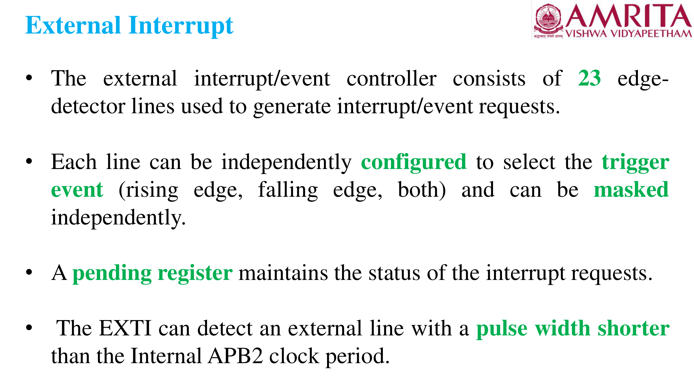
Key Features from Faculty Slides:
- Consists of 23 edge detector lines used to generate interrupt/event requests.
- Each line can be independently configured for trigger events: Rising Edge, Falling Edge, or Both Edges.
- Can be independently masked via Interrupt Mask Register (
EXTI_IMR). - Maintains a pending register (
EXTI_PR) recording active requests. - Can detect input pulses shorter than the Internal APB2 clock period.
Complete Source Code:
#include "stm32f4xx.h"

void EXTI13_Init(void) {
    // 1. Enable clocks for GPIOC, GPIOA (LED), and System Configuration (SYSCFG)
    RCC->AHB1ENR |= RCC_AHB1ENR_GPIOCEN | RCC_AHB1ENR_GPIOAEN;
    RCC->APB2ENR |= RCC_APB2ENR_SYSCFGEN;

    // 2. Set PA5 as Output (LED) and PC13 as Input (Button)
    GPIOA->MODER |= (1U << (5 * 2));
    GPIOC->MODER &= ~(3U << (13 * 2));

    // 3. Select Port C for EXTI13 in SYSCFG_EXTICR4 (bits [7:4] = 0010)
    SYSCFG->EXTICR[3] &= ~(0xFU << 4);
    SYSCFG->EXTICR[3] |=  (0x2U << 4); // 0x2 maps Port C

    // 4. Configure Falling-edge trigger (button press pulls signal Low)
    EXTI->FTSR |= (1U << 13);
    EXTI->RTSR &= ~(1U << 13); // Disable rising edge

    // 5. Unmask interrupt line 13 in IMR
    EXTI->IMR |= (1U << 13);

    // 6. Enable interrupt line in NVIC
    NVIC_SetPriority(EXTI15_10_IRQn, 2);
    NVIC_EnableIRQ(EXTI15_10_IRQn);
}

// Interrupt Service Routine for lines 10 to 15
void EXTI15_10_IRQHandler(void) {
    // Check if line 13 triggered the interrupt
    if (EXTI->PR & (1U << 13)) {
        GPIOA->ODR ^= (1U << 5); // Toggle Green LED
        EXTI->PR = (1U << 13);   // Clear pending bit (WRITE 1 TO CLEAR!)
    }
}📋 Official September 2026 Mid-Term Paper (50 Marks)
Reference Paper SolvedClick on any question below to expand the complete 50/50 model answer, exact circuit schematics, and slide diagram citations:
1. Briefly explain any five advantages of the Cortex-M processors.
Direct Reference: 1 23ECE313_ES_Ch4 Text 1.pdf (Slide 16)
- 1. Low Power Consumption & High Energy Efficiency: Dedicated sleep modes (Sleep, Deep Sleep, Sleep-on-Exit) and the autonomous Wake-up Interrupt Controller (WIC), making it ideal for battery-operated IoT and wearable devices.
- 2. High Performance & Code Density (Thumb-2 Technology): Blends 16-bit and 32-bit instructions to achieve high performance (1.25 DMIPS/MHz) without state-switching penalties or memory bloat.
- 3. Deterministic, Low-Latency Interrupt Handling (Integrated NVIC): Hardware vector fetches, automatic context stacking/unstacking, tail-chaining, and late-arriving preemption achieve a deterministic 12-cycle interrupt latency.
- 4. Comprehensive OS Support: Features dual banked stack pointers (MSP and PSP), two operation modes (Thread and Handler), two privilege levels (Privileged and Unprivileged), SysTick timer, and dedicated OS software exceptions (SVC and PendSV).
- 5. Advanced Debug & Trace Capabilities (CoreSight Architecture): Integrates standard Serial Wire Debug (SWD - 2 pins) and JTAG, hardware breakpoints (FPB), data watchpoints (DWT), and non-intrusive real-time software tracing (ITM/ETM).
2. Assembly Execution, Memory State, IT Block & ICI Bits Trace.
LDR R0, =0x40000000
LDR SP, =0x800000F0
LDR R1, =0x12349876
LDR R2, =0xABCDEF12
MOVS R3, 0x00
IT EQ
STMDB SP!, {R0-R2}
STOP B STOP
Step-by-Step Instruction Execution Trace:
LDR R0, =0x40000000-> R0 =0x40000000.LDR SP, =0x800000F0-> SP =0x800000F0.LDR R1, =0x12349876-> R1 =0x12349876.LDR R2, =0xABCDEF12-> R2 =0xABCDEF12.MOVS R3, 0x00-> Moves 0 into R3. Because the instruction has the 'S' suffix, it updates the condition flags in APSR. Since result is 0, the Z (Zero) flag is set to 1.IT EQ-> If-Then block with condition EQ (Equal / Z == 1). Since Z == 1, the condition evaluates to TRUE. The following instruction executes!STMDB SP!, {R0-R2}-> Store Multiple Decrement Before with write-back (!).- Registers pushed in order: Lowest register number at lowest memory address (Full Descending Stack).
- Total registers = 3 (12 bytes =
0x0C). - Final SP = 0x800000F0 - 0x0C = 0x800000E4.
(a) Contents of Registers R0-R2 and Stack Pointer [2 Marks]:
| Register | Final Value | Explanation |
|---|---|---|
| R0 | 0x40000000 | Unchanged by STMDB |
| R1 | 0x12349876 | Unchanged by STMDB |
| R2 | 0xABCDEF12 | Unchanged by STMDB |
| SP | 0x800000E4 | Decremented by 12 bytes (3 words) |
(b) Contents of Memory Locations from 0x800000E0 to 0x800000F0 [2 Marks]:
| Address | Stored 32-bit Value | Stored Register |
|---|---|---|
0x800000F0 | Unmodified Data | Original SP Base |
0x800000EC | 0xABCDEF12 | R2 (Highest register at highest address) |
0x800000E8 | 0x12349876 | R1 |
0x800000E4 | 0x40000000 | R0 (Lowest register at lowest address) ← New SP |
0x800000E0 | Unmodified Data | Below current SP |
(c) How ICI (Interruptible-Continuable Instruction) is Used [1 Mark]:
(Directly from Slide Deck 1: Ch4 Text 1, Slide 42)
STMDB is a multi-cycle store instruction. If an interrupt occurs halfway through executing STMDB (e.g. after pushing R2 and R1, but before R0), the processor saves the transfer progress into the ICI bits inside the Execution Program Status Register (EPSR). Upon return from the interrupt via EXC_RETURN, the processor inspects the saved ICI bits and resumes execution directly from the remaining transfer (storing R0) instead of restarting the entire instruction from the beginning. This reduces interrupt latency and prevents duplicate bus transactions.
3. Explain how JTAG or SWD facilitates communication between a debug host and Cortex-M3.
Key Points to Write in Exam:
- 1. Physical Pins:
- JTAG (IEEE 1149.1): Uses 4-5 pins (TCK, TMS, TDI, TDO, optional nTRST) to interface with the on-chip Test Access Port (TAP) controller.
- SWD (Serial Wire Debug): ARM alternative requiring only 2 pins:
SWCLK(clock) andSWDIO(bidirectional data), with an optionalSWO(Serial Wire Output) pin for trace data.
- 2. SWJ-DP: On-chip Serial Wire/JTAG Debug Port that detects and switches between JTAG and SWD protocols upon reset.
- 3. DAP (Debug Access Port) Bus: Internal debug bus that translates JTAG/SWD packet commands into internal bus transactions.
- 4. AHB-AP (AHB Access Port): Bridges the DAP directly to the internal AHB System Bus Interconnect.
- 5. Non-Intrusive Live Memory Access: Because AHB-AP is an independent master on the AHB bus matrix, the host debugger can read and write memory, Flash, and peripheral registers on the fly even while the Cortex-M3 core is running at full speed!
4. Explain a scenario where SysTick switches between two tasks with a neat timing diagram.
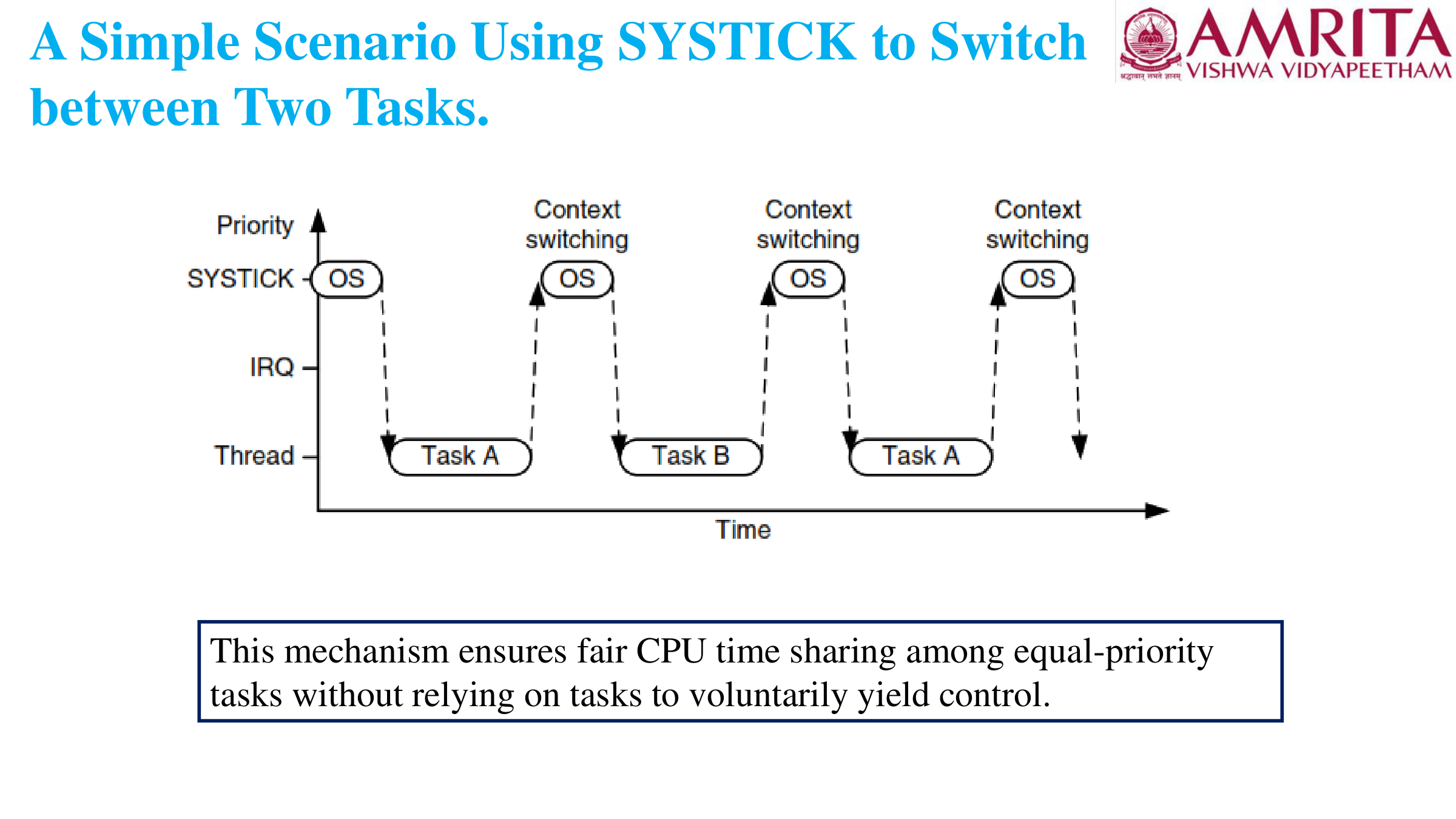
Step-by-Step Context Switching Operation:
- 1. Initial State: Task A is running in Thread mode using the Process Stack Pointer (
PSP). - 2. Timer Expiry: The 24-bit SysTick down-counter reaches 0, sets
COUNTFLAG, and asserts Exception 15 (SysTick). - 3. Automatic Context Save: Hardware automatically pushes caller-saved registers (R0-R3, R12, LR, PC, xPSR) onto Task A's stack (PSP). The processor switches to Handler mode using the Main Stack Pointer (
MSP). - 4. Software Context Save: The SysTick ISR pushes the remaining callee-saved registers (R4-R11) onto Task A's stack and saves Task A's updated SP in its Task Control Block (TCB).
- 5. Scheduler Execution: The OS scheduler selects Task B as the next task to run and retrieves Task B's SP from its TCB.
- 6. Context Restore: Software pops R4-R11 from Task B's stack.
- 7. Exception Exit: Executing
BX LRwithEXC_RETURN = 0xFFFFFFFDtriggers hardware unstacking of R0-R3, R12, LR, PC, xPSR from Task B's stack. The CPU resumes execution of Task B in Thread mode.
5. Explain the interrupt pending and activation behavior with a neat timing diagram.
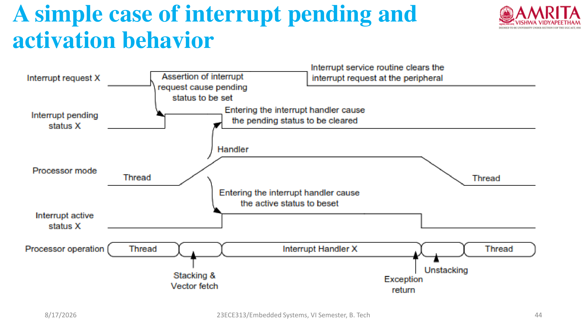
Key Points to Write in Exam:
- 1. Inactive State: The interrupt request signal is de-asserted; interrupt status in NVIC is inactive and not pending.
- 2. Pending State: When a peripheral pulses an interrupt request line, the NVIC latches this into the Interrupt Set-Pending Register (
NVIC_ISPR). The interrupt is now Pending. - 3. Arbitration & Acceptance: The processor accepts the pending interrupt if:
- The interrupt is enabled in
NVIC_ISER. - Its priority is higher than the currently executing context and the
BASEPRI/PRIMASKregisters.
- The interrupt is enabled in
- 4. Active State: When the core enters the exception entrance sequence (stacking), hardware automatically transitions the interrupt from Pending to Active. The pending flag is cleared unless a new pulse has arrived.
- 5. Multiple Pulses Latching: If multiple request pulses occur while the interrupt is already pending or active, the NVIC latches the pending state only once, ensuring exactly one subsequent ISR execution.
6. Explain the problem associated with context switching during an IRQ with a neat timing diagram.
Detailed Operational Explanation:
- Scenario: Task A is executing normally in Thread mode. A periodic SysTick timer interrupt triggers to initiate a task switch.
- The Conflict: While the SysTick handler is executing the context switch sequence, an urgent external peripheral interrupt (e.g., UART communication or Motor Control IRQ) arrives.
- The Failure: Because the processor is already executing inside an ISR (SysTick handler), and both have equal or configurable priorities, the external IRQ is blocked and delayed until the lengthy context switch operation completes.
- Consequence: Crucial real-time peripheral deadlines are missed, creating unacceptable interrupt latency.
- The Solution (PendSV): To resolve this, the OS delegates context switching to the Pendable Service Call (PendSV), which is programmed to the lowest possible interrupt priority. SysTick simply sets the
PENDSVSETbit and exits immediately, allowing the external IRQ to run with zero delay. PendSV executes only after all pending IRQs complete!
7. How does the Wake-Up Interrupt Controller (WIC) help in low-power deep sleep? Explain the sequence.
Sequence of Events:
- Entering Deep Sleep: Software sets
SLEEPDEEPinSCRand executesWFI. - Clock Gating: The Power Management Unit (PMU) shuts down high-speed system oscillators, gating clocks to the core and NVIC (NVIC is completely powered down).
- WIC Monitoring: The Wake-Up Interrupt Controller (WIC) remains active in an ultra-low-power, always-on voltage domain, mirroring the enabled interrupt lines.
- External Event Detection: An external interrupt signal arrives at a pin. The WIC detects the signal edge/level.
- Waking PMU: The WIC asserts a wake-up signal to the Power Management Unit (PMU).
- Restoring Clocks: The PMU restarts oscillators and restores power to the core and NVIC.
- NVIC Vectoring: The NVIC resumes normal operation, detects the pending interrupt, and vectors the core to execute the ISR.
8. C Program & Circuit to generate 3V average output from 5V DC supply via STM32 PWM.
Supply Voltage V_supply = 5.0 V. Target Average Voltage V_avg = 3.0 V.
Duty Cycle D = V_avg / V_supply = 3.0 V / 5.0 V = 0.60 = 60%.
Using STM32F446RE Timer 2 Channel 1 on Pin PA5 (16 MHz clock, 1 kHz PWM frequency):
• PSC = 0 -> Timer Clock = 16 MHz.
• ARR = 15999 -> f_PWM = 16 MHz / 16000 = 1 kHz.
• CCR1 = 60% * 16000 = 9600.
Circuit Interfacing Diagram:
Complete Embedded C Program:
#include "stm32f4xx.h"

int main(void) {
    // 1. Enable AHB1 clock for GPIOA and APB1 clock for TIM2
    RCC->AHB1ENR |= RCC_AHB1ENR_GPIOAEN;
    RCC->APB1ENR |= RCC_APB1ENR_TIM2EN;

    // 2. Configure PA5 as Alternate Function Mode ('10')
    GPIOA->MODER &= ~(3U << (5 * 2));
    GPIOA->MODER |=  (2U << (5 * 2));

    // 3. Connect PA5 to AF1 (TIM2_CH1) via AFR[0] (Bits [23:20] = 0001)
    GPIOA->AFR[0] &= ~(0xFU << (5 * 4));
    GPIOA->AFR[0] |=  (1U << (5 * 4)); // 0x1 selects AF1

    // 4. Set Timebase: 1 kHz PWM frequency at 16 MHz clock
    TIM2->PSC = 0;     // Clock = 16 MHz
    TIM2->ARR = 15999; // Period = 16 MHz / 16000 = 1 ms (1 kHz)

    // 5. Set 60% Duty Cycle for 3V average output from 5V supply: CCR1 = 9600
    TIM2->CCR1 = 9600;

    // 6. Configure Channel 1 for PWM Mode 1 (OC1M = 110) with Preload Enable
    TIM2->CCMR1 |= (6U << 4) | TIM_CCMR1_OC1PE;

    // 7. Enable Output on Channel 1
    TIM2->CCER |= TIM_CCER_CC1E;

    // 8. Enable Auto-Reload Preload and start counter
    TIM2->CR1 |= TIM_CR1_ARPE | TIM_CR1_CEN;

    while (1) {
        // Continuous 60% PWM waveform generated autonomously by hardware
    }
}
9. Analog Sensor (PA0), Relay Fan (PA5), ADC 12-Bit, UART Serial Monitor + Circuit.
Reference Voltage V_REF = 3.3 V, 12-bit ADC Resolution -> 4095 levels.
Threshold Voltage = 2.2 V.
Threshold Digital Code = (2.2 V / 3.3 V) * 4095 = (2/3) * 4095 = 2730.
Control Logic: When ADC >= 2730 (V >= 2.2 V), turn ON Relay on PA5. When ADC < 2730 (V < 2.2 V), turn OFF Relay.
Circuit Interfacing Diagram:
Complete Embedded C Program:
#include "stm32f4xx.h"
#include

void USART2_Init(void);
void USART2_SendChar(char c);
void USART2_SendString(char *str);
void ADC1_PA0_Init(void);
uint32_t ADC1_Read(void);

void delay_ms(uint32_t ms) {
    uint32_t count = (SystemCoreClock / 10000) * ms;
    for (volatile uint32_t i = 0; i < count; i++) { __NOP(); }
}

int main(void) {
    char buffer[80];
    uint32_t adc_val = 0;
    float voltage = 0.0f;

    // 1. Initialize Peripherals
    USART2_Init();
    ADC1_PA0_Init();

    // 2. Configure PA5 as General Output for Relay Control
    RCC->AHB1ENR |= RCC_AHB1ENR_GPIOAEN;
    GPIOA->MODER &= ~(3U << (5 * 2));
    GPIOA->MODER |=  (1U << (5 * 2)); // Output mode '01'

    USART2_SendString("--- Sensor & Relay Monitoring System Online ---
");

    while (1) {
        // Read 12-bit ADC value
        adc_val = ADC1_Read();

        // Convert code to voltage: V = (ADC / 4095) * 3.3
        voltage = ((float)adc_val / 4095.0f) * 3.3f;

        // Relay Control Logic: Threshold 2.2V corresponds to code 2730
        if (adc_val >= 2730) {
            GPIOA->ODR |= (1U << 5); // Relay ON (Fan runs)
        } else {
            GPIOA->ODR &= ~(1U << 5); // Relay OFF (Fan stopped)
        }

        // Transmit readings over UART to PuTTY Serial Monitor
        snprintf(buffer, sizeof(buffer), "ADC: %lu | Volt: %.2f V | Fan: %s
",
                 adc_val, voltage, (adc_val >= 2730) ? "ON" : "OFF");
        USART2_SendString(buffer);

        delay_ms(500); // 500 ms sampling period
    }
}

// USART2 Configuration: PA2 as TX (AF7), 9600 Baud at 16 MHz
void USART2_Init(void) {
    RCC->AHB1ENR |= RCC_AHB1ENR_GPIOAEN;
    RCC->APB1ENR |= RCC_APB1ENR_USART2EN;

    GPIOA->MODER &= ~(3U << (2 * 2));
    GPIOA->MODER |=  (2U << (2 * 2)); // Alternate Function '10'

    GPIOA->AFR[0] &= ~(0xFU << (2 * 4));
    GPIOA->AFR[0] |=  (7U << (2 * 4)); // AF7 for USART2

    USART2->BRR = 0x0683; // 9600 Baud at 16 MHz
    USART2->CR1 = USART_CR1_TE | USART_CR1_UE; // Transmitter Enable & Module Enable
}

void USART2_SendChar(char c) {
    while (!(USART2->SR & USART_SR_TXE)); // Wait for TX data register empty
    USART2->DR = c;
}

void USART2_SendString(char *str) {
    while (*str) { USART2_SendChar(*str++); }
}

// ADC1 Configuration on PA0 (Channel 0)
void ADC1_PA0_Init(void) {
    RCC->AHB1ENR |= RCC_AHB1ENR_GPIOAEN;
    RCC->APB2ENR |= RCC_APB2ENR_ADC1EN;

    GPIOA->MODER |= (3U << (0 * 2)); // PA0 Analog Mode '11'

    ADC1->SQR1 = 0; // 1 conversion
    ADC1->SQR3 = 0; // Channel 0 first

    // Sample time: 84 cycles for Channel 0 (SMPR2 bits [2:0] = 100)
    ADC1->SMPR2 |= (4U << 0);

    ADC1->CR2 |= ADC_CR2_ADON; // Power ON ADC
}

uint32_t ADC1_Read(void) {
    ADC1->CR2 |= ADC_CR2_SWSTART;     // Trigger conversion
    while (!(ADC1->SR & ADC_SR_EOC)); // Wait for End Of Conversion
    return ADC1->DR;                  // Read 12-bit value (clears EOC)
}
📝 Practice Question Paper - Set 1 (50 Marks)
Model Exam Set 1Mirroring the exact difficulty, BTL taxonomy, and question pattern of Professor Giriraja C. V. Click to reveal complete solutions and slide citations:
1. Briefly explain the four Memory Access Attributes in Cortex-M3 architecture.
Direct Reference: 2 23ECE313_ES_Ch_Txt1.pdf (Slide 11)
- 1. Bufferable: Write transfers to memory can be handled by an internal write buffer while the processor continues executing subsequent instructions without stalling. (Nuance: Write buffers can cause Imprecise Bus Faults if the bus later returns an error!)
- 2. Cacheable: Data or instruction reads from memory can be copied into high-speed local cache memories to accelerate subsequent accesses.
- 3. Executable (XN - Execute Never): Defines whether instructions can be fetched and executed from the region. Attempting to fetch code from an XN region (like Peripherals or System Space) triggers an immediate MemManage Fault.
- 4. Shareable: Indicates that memory is accessible by multiple bus masters (e.g. DMA and CPU core). The memory system enforces hardware coherency protocols across shared masters.
2. Assembly Execution, Reverse Subtract, IT Block & Full Descending Stack Trace.
LDR R0, =0x20000000
LDR SP, =0x20000200
LDR R1, =0x11223344
LDR R2, =0x55667788
SUBS R3, R1, R2
IT MI
STMDB SP!, {R0, R2}
STOP B STOP
Step-by-Step Execution Analysis:
LDR R0, =0x20000000-> R0 =0x20000000.LDR SP, =0x20000200-> SP =0x20000200.LDR R1, =0x11223344-> R1 =0x11223344.LDR R2, =0x55667788-> R2 =0x55667788.SUBS R3, R1, R2-> Subtracts R2 from R1. Since R1 < R2, the result is negative. The N (Negative) flag in APSR is set to 1.IT MI-> If-Then block with condition MI (Minus / Negative: N == 1). Since N = 1, condition evaluates to TRUE.STMDB SP!, {R0, R2}-> Pushes 2 registers (8 bytes = 0x08).- Final SP = 0x20000200 - 0x08 = 0x200001F8.
- R2 is placed at
0x200001FC, R0 is placed at0x200001F8.
Final State:
| Register / Address | Value |
|---|---|
| R0 | 0x20000000 |
| R1 | 0x11223344 |
| R2 | 0x55667788 |
| SP | 0x200001F8 |
0x200001FC | 0x55667788 (R2) |
0x200001F8 | 0x20000000 (R0) |
3. Explain the CoreSight On-Chip Debug Architecture and Differentiate Halt vs Debug Monitor Modes.
Functions of Key CoreSight Units:
- DWT (Data Watchpoint and Trace): Monitors data address accesses, provides cycle counting, and event profiling.
- FPB (Flash Patch and Breakpoint): Hardware breakpoint comparator (6 instruction breakpoints, 2 literal slots).
- ITM (Instrumentation Trace Macrocell): Software printf debugging via Serial Wire Output (SWO) pin.
- ETM (Embedded Trace Macrocell): Instruction tracing streamed out via TPIU.
Comparison of Debug Modes:
| Feature | Halt Mode | Debug Monitor Mode |
|---|---|---|
| CPU State | Completely stopped (halted) | Executes Exception 12 handler |
| SysTick Timer | Stopped | Continues running |
| Interrupts | Masked/pended | Higher-priority interrupts can still preempt |
| Application | Bare-metal firmware debugging | Safety-critical motor control / RTOS |
4. With a neat timing diagram, explain the Cortex-M3 Reset Sequence and initial vector fetches.
Step-by-Step Reset Sequence:
- Step 1: System reset signal is de-asserted; clock stabilizes.
- Step 2 (Fetch Vector 0): Hardware fetches the 32-bit word from memory address
0x00000000and loads it directly into the Main Stack Pointer (MSP). This ensures a valid stack exists before executing any code! - Step 3 (Fetch Vector 1): Hardware fetches the 32-bit word from memory address
0x00000004and loads it directly into the Program Counter (PC). This word contains the address of theReset_Handlerfunction. Bit 0 of this address must be1to specify Thumb state. - Step 4: Processor begins instruction execution at
Reset_Handlerin Privileged Thread Mode.
5. With a neat diagram, explain Preempt Priority and Sub-Priority splitting in the NVIC.
Priority Rules:
- Each interrupt priority level register holds an 8-bit priority value (microcontrollers implement top 3 to 8 bits). Smaller numerical values indicate higher logical priority (0 is highest).
- The
PRIGROUPfield in the Application Interrupt and Reset Control Register (AIRCR) splits the priority bits into two fields:- Preemption Priority: Determines whether an arriving interrupt can interrupt (nest inside) an currently executing ISR.
- Sub-Priority: When two pending interrupts have the identical preemption priority, the one with the smaller sub-priority value executes first. Sub-priority does NOT cause preemption!
6. Explain the 4 Fault Exceptions in Cortex-M3 and Fault Escalation to HardFault.
Fault Descriptions:
- MemManage (Exc #4): MPU permission violation, unprivileged task accessing privileged memory, or executing from Execute-Never (XN) regions.
- Bus Fault (Exc #5): Bus error response during read/write. Precise (immediate) vs Imprecise (buffered write).
- Usage Fault (Exc #6): Undefined instruction, division by zero, unaligned memory access, or clearing Thumb bit (T=0).
- HardFault (Exc #3): Fixed priority -1. Caused by:
- Fault Escalation: When a configurable fault occurs while its handler is disabled in
SHCSR. - A fault occurring inside an active fault handler with equal or higher priority.
- Bus error during vector table fetch.
- Fault Escalation: When a configurable fault occurs while its handler is disabled in
7. Explain Sleep-on-Exit and Multiprocessor Synchronization (SEV & WFE) with neat flowcharts.
Sleep-on-Exit Working:
Configured by setting SLEEPONEXIT in System Control Register (SCR). After ISR completes, the processor skips Thread Mode and returns directly to sleep, eliminating stack restore overhead in interrupt-only systems.
Multiprocessor Signals:
SEV instruction pulses TXEV pin to wake other cores. WFE (Wait For Event) sleeps until RXEV is asserted.
8. C Program & Circuit to generate an accurate 2-second delay using TIM5 to toggle an LED on PA5.
Clock f_sys = 16 MHz. Prescaler PSC = 15999 -> f_timer = 16 MHz / 16000 = 1 kHz (1 ms tick).
For 2 seconds: ARR = (2 * 1000) - 1 = 1999.
Circuit Interfacing Diagram:
Complete Embedded C Code:
#include "stm32f4xx.h"

void delay_seconds(uint32_t seconds) {
    RCC->APB1ENR |= RCC_APB1ENR_TIM5EN; // Enable TIM5 clock
    TIM5->PSC = 15999;                  // 1 ms tick (16 MHz / 16000)
    TIM5->ARR = (seconds * 1000) - 1;   // Reload value
    TIM5->CNT = 0;                      // Reset count
    TIM5->CR1 |= TIM_CR1_CEN;           // Start timer
    while (!(TIM5->SR & TIM_SR_UIF));   // Wait for overflow UIF flag
    TIM5->SR  &= ~TIM_SR_UIF;           // Clear flag
    TIM5->CR1 &= ~TIM_CR1_CEN;          // Stop timer
}

int main(void) {
    RCC->AHB1ENR |= RCC_AHB1ENR_GPIOAEN;
    GPIOA->MODER &= ~(3U << (5 * 2));
    GPIOA->MODER |=  (1U << (5 * 2)); // Output mode '01'

    while (1) {
        GPIOA->ODR ^= (1U << 5); // Toggle LED
        delay_seconds(2);        // 2-second delay
    }
}
9. External Interrupt (EXTI13) System Design on PC13 toggling LED on PA5 + Circuit Diagram.
Circuit Interfacing Diagram:
Complete Embedded C Program:
#include "stm32f4xx.h"

void EXTI13_Init(void) {
    // 1. Enable Clocks for GPIOA (LED), GPIOC (Button), and SYSCFG
    RCC->AHB1ENR |= RCC_AHB1ENR_GPIOAEN | RCC_AHB1ENR_GPIOCEN;
    RCC->APB2ENR |= RCC_APB2ENR_SYSCFGEN;

    // 2. PA5 as Output (LED), PC13 as Input (Button)
    GPIOA->MODER |= (1U << (5 * 2));
    GPIOC->MODER &= ~(3U << (13 * 2));

    // 3. Connect EXTI13 to Port C in SYSCFG_EXTICR4 (bits [7:4] = 0010)
    SYSCFG->EXTICR[3] &= ~(0xFU << 4);
    SYSCFG->EXTICR[3] |=  (0x2U << 4); // Port C

    // 4. Configure Falling-edge Trigger in FTSR (Button press pulls to 0)
    EXTI->FTSR |= (1U << 13);
    EXTI->RTSR &= ~(1U << 13);

    // 5. Unmask interrupt line 13 in IMR
    EXTI->IMR |= (1U << 13);

    // 6. Enable in NVIC
    NVIC_SetPriority(EXTI15_10_IRQn, 2);
    NVIC_EnableIRQ(EXTI15_10_IRQn);
}

void EXTI15_10_IRQHandler(void) {
    if (EXTI->PR & (1U << 13)) {
        GPIOA->ODR ^= (1U << 5); // Toggle LED
        EXTI->PR = (1U << 13);   // Clear pending bit (WRITE 1 TO CLEAR!)
    }
}

int main(void) {
    EXTI13_Init();
    while (1) {
        __WFI(); // Sleep until button press interrupt
    }
}
📝 Practice Question Paper - Set 2 (50 Marks)
Model Exam Set 2Comprehensive coverage of Unit 1, Unit 2, and Peripheral Interfacing. Click any question to reveal complete step-by-step solutions, slide citations, register breakdowns, and schematics:
1. Explain the Operating Modes (Thread vs Handler), Privilege Levels, and Dual Stack Pointers (MSP vs PSP) with the CONTROL Register.
Direct Reference: 1 23ECE313_ES_Ch4 Text 1.pdf (Slides 19, 23, 27)
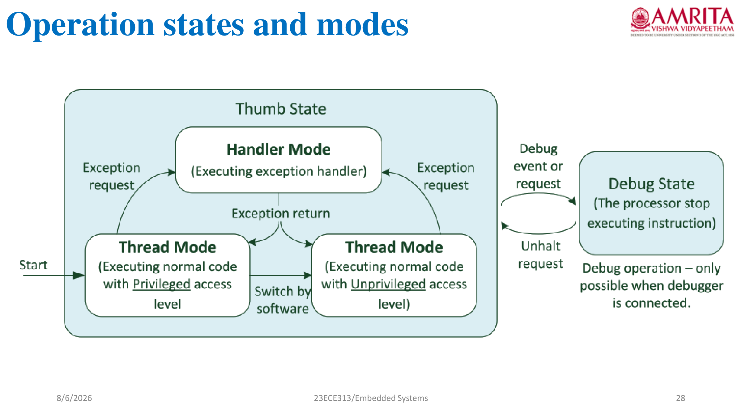
1. Two Operating Modes:
- Thread Mode: The default mode entered upon reset. Used to execute regular application tasks / main program code. Can run in either Privileged or Unprivileged state.
- Handler Mode: Automatically entered whenever an exception or interrupt occurs. Always executes in Privileged state (cannot be switched to unprivileged). Returns to Thread mode upon exception completion via
EXC_RETURN.
2. Two Privilege Levels:
- Privileged Level: Software has full access to all memory ranges and all core control registers (NVIC, MPU, SCB, SysTick). Allowed to switch to unprivileged state by modifying the CONTROL register.
- Unprivileged (User) Level: Restricts software from accessing System Control Space (PPB:
0xE0000000 - 0xE00FFFFF), and restricts MPU regions marked privileged-only. Prevents user bugs from crashing the operating system. Cannot directly switch back to privileged mode; must execute anSVC(Supervisory Call).
3. The CONTROL Register (Bits [1:0]):
- CONTROL[0] (nPRIV):
0= Privileged thread execution.1= Unprivileged thread execution.
- CONTROL[1] (SPSEL):
0= Use Main Stack Pointer (MSP) in Thread mode.1= Use Process Stack Pointer (PSP) in Thread mode.- Note: Handler mode always uses MSP regardless of SPSEL setting!
4. Dual Stack Pointers (MSP vs PSP):
- MSP (Main Stack Pointer): Used by the OS kernel, exception handlers, and interrupts. Configured at boot from vector table index 0 (`0x00000000`).
- PSP (Process Stack Pointer): Dedicated stack pointer assigned to individual user application tasks in an RTOS.
- Key Advantage: If a user task overflows its stack (PSP), the system kernel and interrupt handlers (using MSP) remain completely uncorrupted and can safely catch the fault!
2. Derive the Bit-Banding memory mapping formula. Calculate the exact alias address for Bit 5 of GPIOA_ODR (0x40020014) and explain its real-time advantages.
Direct Reference: 2 23ECE313_ES_Ch_Txt1.pdf (Slide 12)
1. Mathematical Derivation of the Formula:
Cortex-M3 provides two 1 MB bit-band regions mapped to 32 MB alias regions:
- SRAM Bit-Band:
0x20000000 - 0x200FFFFF──► Alias:0x22000000 - 0x23FFFFFF - Peripheral Bit-Band:
0x40000000 - 0x400FFFFF──► Alias:0x42000000 - 0x43FFFFFF
In the alias region, every single bit in the bit-band region is mapped to an entire 32-bit (4-byte) word. Therefore:
- 1 byte in the bit-band region contains 8 bits, requiring
8 × 4 = 32 bytesin the alias region. - Each individual bit n within that byte is offset by
n × 4 bytes.
Bit_Word_Addr = Alias_Base + (Byte_Offset × 32) + (Bit_Number × 4)Where:
Byte_Offset = Target_Address - Bit_Band_Base
2. Step-by-Step Numerical Calculation for Bit 5 of GPIOA_ODR (0x40020014):
- Target Address:
0x40020014(Peripheral Region) - Bit Number (n):
5 - Peripheral Base:
0x40000000 - Peripheral Alias Base:
0x42000000 - Byte Offset:
0x40020014 - 0x40000000 = 0x00020014(in decimal: 131,092 bytes) - Calculate (Byte_Offset × 32):
Multiplying by 32 in hex is shifting left by 5 bits:0x00020014 × 0x20 = 0x00400280(decimal: 131,092 × 32 = 4,194,944 = 0x400280) - Calculate (Bit_Number × 4):
5 × 4 = 20 = 0x00000014 - Total Alias Address:
0x42000000 + 0x00400280 + 0x00000014 = 0x42400294
0x42400294. Writing 1 to this address sets PA5; writing 0 clears PA5.
3. Real-Time & Multitasking Advantages:
- Atomic Operation: Performs atomic read-modify-write entirely in hardware without disabling interrupts.
- Eliminates Race Conditions: If an interrupt occurs between a read and write of a shared port register, software bit operations (
ODR |= (1<<5)) corrupt adjacent bits. Bit-banding prevents this completely! - Code Density & Speed: Replaces 3 assembly instructions (
LDR,ORR,STR) with a single atomicSTRinstruction.
3. Contrast Precise vs Imprecise Bus Faults. Explain the Write Buffer mechanism and how to diagnose imprecise faults using ACTLR.
Direct Reference: 3 23ECE313_ES_Ch12_Txt1.pdf (Slides 10–14, 23)
| Feature | Precise Bus Fault | Imprecise Bus Fault |
|---|---|---|
| Cause | Synchronous bus error (Instruction fetch, data read, or non-buffered write). | Asynchronous bus error caused by the Write Buffer during buffered writes. |
| Stacked PC Value | Exact: Stacked PC points directly to the instruction that triggered the bus error. | Inaccurate: The processor moved on while the write buffer was writing. Stacked PC points to an arbitrary later instruction! |
| Fault Address Register (BFAR) | Valid: BFSR->BFARVALID = 1. BFAR register contains the exact faulting memory address. |
Invalid: BFSR->BFARVALID = 0. The memory address that triggered the fault is lost. |
| Status Flag in BFSR | PRECISERR (Bit 1) = 1 |
IMPRECISERR (Bit 2) = 1 |
Mechanism of the Imprecise Bus Fault (The Write Buffer Trap):
To maximize execution throughput, Cortex-M incorporates an internal Write Buffer on the system bus. When a program writes to memory, the write data is queued in the buffer, and the CPU immediately proceeds to execute subsequent instructions without waiting for bus acknowledgement. If the bus later rejects the transaction (e.g. invalid peripheral address, slave timeout), the error arrives cycles later. By then, the CPU is already executing unrelated code!
Diagnostic Method using ACTLR (Auxiliary Control Register):
Because imprecise bus faults make debugging nearly impossible (unknown PC and unknown address), ARM provides a hardware override:
// Set DISDEFWBUF bit (Bit 1) in ACTLR (Address: 0xE000E008)
SCB->ACTLR |= SCB_ACTLR_DISDEFWBUF_Msk; // Disables Write Buffer
Effect: Disabling the write buffer forces all write operations to complete synchronously before the next instruction executes. When the faulty write occurs, it immediately triggers a Precise Bus Fault, allowing the developer to inspect the exact stacked PC and read the faulty address from BFAR!
4. With a neat timing diagram, explain the 3-Stage Pipeline in Cortex-M3 and analyze the Branch Flush penalty.
Direct Reference: 1 23ECE313_ES_Ch4 Text 1.pdf (Slide 17)
1. The Three Pipeline Stages:
- Stage 1 (Fetch): Fetches the 16-bit or 32-bit Thumb-2 instruction from memory (Flash/SRAM) via the I-Code or System bus and places it into the instruction buffer.
- Stage 2 (Decode): Decodes the instruction opcode, identifies register operands, and generates internal datapath control signals.
- Stage 3 (Execute): Executes the operation in the ALU, performs barrel shifter operations, updates status flags, or accesses memory (Load/Store).
2. Normal Sequential Execution (1 Instruction per Cycle Throughput):
Clock Cycle:     | T1 | T2 | T3 | T4 | T5 |
Instr 1 (ADD):   | Fe | De | Ex |    |    |
Instr 2 (SUB):   |    | Fe | De | Ex |    |
Instr 3 (MOV):   |    |    | Fe | De | Ex |
3. Branch Hazard & Pipeline Flush Penalty:
When a branch instruction (e.g., B label, BL, BX) reaches the Execute stage and the branch is taken, the instructions already fetched and decoded in stages 1 and 2 are invalid and must be flushed (discarded).
Clock Cycle:       | T1 | T2 | T3   | T4    | T5    |
Instr 1 (B target):| Fe | De | Ex   |       |       |  <-- Branch target computed in Ex
Instr 2 (Next):    |    | Fe | De   | FLUSH |       |  <-- Discarded!
Instr 3 (Next+1):  |    |    | Fe   | FLUSH |       |  <-- Discarded!
Target Instr 1:    |    |    |      | Fe    | De    | Ex  <-- 2 cycle branch penalty!
4. Mitigation in Cortex-M Architecture:
- Branch Speculation: Speculative prefetching fetches the target address early.
- Thumb-2 IT (If-Then) Blocks: Conditional execution allows up to 4 instructions to execute conditionally without taking a branch, completely eliminating branch flush penalties in short decision trees!
5. Explain the Supervisory Call (SVC) exception mechanism, hardware stack frame, and how the C handler extracts the SVC immediate number.
Direct Reference: 3 23ECE313_ES_Ch12_Txt1.pdf (Slides 28–34)
1. Purpose of SVC:
The SVC (Supervisory Call) instruction generates a synchronous software exception used by unprivileged user application tasks to request privileged operating system services (file system, hardware drivers, memory allocation).
2. Step-by-Step Hardware Execution:
- User task executes
SVC #number(e.g.SVC #3). - Hardware automatically saves the standard 8-word stack frame on the current stack (PSP):
[SP+0] = R0, [SP+4] = R1, [SP+8] = R2, [SP+12] = R3, [SP+16] = R12, [SP+20] = LR, [SP+24] = Return PC, [SP+28] = xPSR. - Processor switches to Handler Mode (Privileged) and loads
EXC_RETURNintoLR. - Processor branches to
SVC_Handlerusing the vector fetched from vector table entry 11 (offset0x0000002C).
3. Assembly Trampoline to Detect Stack Pointer (MSP vs PSP):
__asm void SVC_Handler(void) {
    TST LR, #4          // Test Bit 2 of EXC_RETURN (0 = MSP, 1 = PSP)
    ITE EQ
    MRSEQ R0, MSP       // Stack pointer was MSP, pass in R0
    MRSNE R0, PSP       // Stack pointer was PSP, pass in R0
    B SVC_Handler_C     // Branch to C handler with stack frame pointer in R0
}
4. Extracting the SVC Number in C:
void SVC_Handler_C(uint32_t *svc_args) {
    // svc_args[6] is the stacked Return PC!
    // Since Thumb-2 SVC is a 2-byte opcode [0xDF, SVC_#],
    // subtract 2 bytes from Return PC to point directly to the SVC instruction!
    uint8_t svc_number = ((uint8_t *)svc_args[6])[-2];

    switch (svc_number) {
        case 0: // Read Service
            svc_args[0] = OS_Read(svc_args[1], svc_args[2]); // Return in R0
            break;
        case 1: // Write Service
            svc_args[0] = OS_Write(svc_args[1], svc_args[2]);
            break;
        default:
            break;
    }
}svc_args[0] (stacked R0), which hardware automatically restores into register R0 upon unstacking!
6. Compare the Interrupt Masking Registers: PRIMASK, FAULTMASK, and BASEPRI. Write the assembly instructions to control them.
Direct Reference: 1 23ECE313_ES_Ch4 Text 1.pdf (Slides 31–33)
| Register | Width | Effective Priority Level | Exceptions Blocked | Assembly Instructions |
|---|---|---|---|---|
| PRIMASK | 1 bit | 0 (Highest configurable priority) | Blocks all interrupts with configurable priority. NMI and HardFault still execute! | CPSID i (Disable IRQs)CPSIE i (Enable IRQs) |
| FAULTMASK | 1 bit | -1 (HardFault priority level) | Blocks all interrupts and all configurable faults (MemManage, BusFault, UsageFault) plus HardFault. Only NMI can execute! Cleared automatically on exception exit. | CPSID f (Disable All)CPSIE f (Enable All) |
| BASEPRI | Up to 8 bits | Configurable threshold N | Blocks only interrupts with priority level ≥ N (numerically equal or lower priority). Leaves higher priority interrupts (< N) active. When set to 0, masking is disabled. | MSR BASEPRI, R0MRS R0, BASEPRI |
Why RTOS Kernels Prefer BASEPRI over PRIMASK:
In hard real-time systems, critical tasks (e.g. emergency motor stop, radar timing) must never experience interrupt latency. By setting BASEPRI to a mid-level threshold (e.g. priority 3), the OS scheduler can protect its internal queues without blocking ultra-high-priority hard real-time interrupts (priorities 0, 1, and 2)!
7. Explain the NVIC Advanced Mechanisms: Tail-Chaining and Late-Arrival with cycle-accurate timing comparisons.
Direct Reference: 2 23ECE313_ES_Ch_Txt1.pdf (Slides 25–28)
1. Tail-Chaining Mechanism:
Occurs when an interrupt arrives while the processor is already servicing another interrupt, or during the completion phase of an ISR.
- Traditional Microcontroller Flow: Unstacking previous registers (16 cycles) ──► Re-stacking registers for next interrupt (16 cycles) = 32+ clock cycles wasted!
- Cortex-M3 Tail-Chaining Flow: The NVIC skips the unstacking and re-stacking completely! It reuses the existing stack frame and transitions directly from the finishing ISR to the pending ISR in just 6 clock cycles.
Traditional: [ ISR 1 ] ──► [ Unstack (16c) ] ──► [ Restack (16c) ] ──► [ ISR 2 ] (32+ cycles)
Cortex-M3:   [ ISR 1 ] ──► [ Tail-Chain (6 cycles) ] ───────────────► [ ISR 2 ] (6 cycles!)
2. Late-Arrival Mechanism:
Occurs when a higher-priority interrupt arrives while the processor is in the middle of stacking registers for an earlier, lower-priority interrupt.
- Behavior: The processor does NOT abort or restart the stacking process. It completes the 12-cycle register stacking in progress, updates the vector fetch address to point to the higher-priority interrupt handler, and enters the high-priority ISR immediately!
- Result: Zero cycles wasted. When the high-priority ISR completes, the original lower-priority interrupt is serviced immediately via tail-chaining in 6 cycles.
8. Hardware Interfacing & C Program to generate a 10 kHz PWM signal with 75% duty cycle on PA5 (TIM2_CH1) to drive a DC motor via MOSFET.
Direct Reference: STM32F446RE_Timers_PWM_ADC_Mazidi.pdf (Slides 4–9)
1. Circuit Interfacing Schematic:
2. Mathematical Calculations (System Clock = 16 MHz HSI):
- Target PWM Frequency:
f_PWM = 10 kHz - Timer Clock:
16 MHz - Set Prescaler:
PSC = 0(Counter frequency = 16 MHz / 1 = 16 MHz) - Calculate Auto-Reload:
ARR = (16,000,000 / 10,000) - 1 = 1600 - 1 = 1599 - Duty Cycle (75%):
CCR1 = 0.75 × (ARR + 1) = 0.75 × 1600 = 1200
3. Complete CMSIS Register C Program:
#include "stm32f4xx.h"

void PWM_TIM2_PA5_Init(void) {
    // 1. Enable Clock for GPIOA (AHB1) and TIM2 (APB1)
    RCC->AHB1ENR |= RCC_AHB1ENR_GPIOAEN;
    RCC->APB1ENR |= RCC_APB1ENR_TIM2EN;

    // 2. Configure PA5 as Alternate Function mode (MODER bits [11:10] = '10')
    GPIOA->MODER &= ~(3U << (5 * 2));
    GPIOA->MODER |=  (2U << (5 * 2));

    // 3. Set Alternate Function to AF1 (TIM2_CH1) in AFR[0] (Bits [23:20] = 0x01)
    GPIOA->AFR[0] &= ~(0xFU << (5 * 4));
    GPIOA->AFR[0] |=  (1U   << (5 * 4));

    // 4. Configure TIM2 Time Base: 10 kHz
    TIM2->PSC = 0;       // Prescaler = 0 (16 MHz timer clock)
    TIM2->ARR = 1599;    // Auto-reload value (Period = 1600 cycles = 100 us)

    // 5. Configure 75% Duty Cycle
    TIM2->CCR1 = 1200;   // Compare match value (75% of 1600)

    // 6. Set PWM Mode 1 (OC1M = '110') and enable Preload (OC1PE = 1) in CCMR1
    TIM2->CCMR1 &= ~(7U << 4);
    TIM2->CCMR1 |=  (6U << 4);   // PWM Mode 1: High until counter > CCR1
    TIM2->CCMR1 |=  TIM_CCMR1_OC1PE;

    // 7. Enable Channel 1 Output in CCER (CC1E = 1, Active High polarity)
    TIM2->CCER |= TIM_CCER_CC1E;

    // 8. Enable Main Counter in CR1 (CEN = 1)
    TIM2->CR1 |= TIM_CR1_CEN;
}

int main(void) {
    PWM_TIM2_PA5_Init();
    while (1) {
        // Hardware timer generates 10 kHz 75% PWM automatically!
    }
}
9. Interfacing & C Program: Read analog temperature on PA0 (ADC1), trigger 12V cooling fan on PA5 when V > 2.0V, and send serial alert over USART2 at 115200 baud.
Direct Reference: STM32F446RE_Timers_PWM_ADC_Mazidi.pdf (Slides 11–17)
1. Complete Circuit Interfacing Diagram:
2. Mathematical Calculations:
- ADC Resolution: 12-bit (0 to 4095 counts for 0V to 3.3V).
- Quantization Step:
3.3V / 4095 ≈ 0.8058 mV/count. - Threshold Voltage:
V_th = 2.0V. - Threshold Digital Count:
Threshold = (2.0V / 3.3V) × 4095 = 2481.8 ≈ 2482. - USART2 Baud Rate:
16 MHz / (16 × 115200) = 8.6805.
Mantissa = 8 =0x08, Fraction =0.6805 × 16 ≈ 11 = 0x0B.USART2->BRR = 0x008B.
3. Complete Embedded C Program:
#include "stm32f4xx.h"

void System_Init(void) {
    // 1. Enable Peripheral Clocks
    RCC->AHB1ENR |= RCC_AHB1ENR_GPIOAEN;  // GPIOA clock
    RCC->APB2ENR |= RCC_APB2ENR_ADC1EN;   // ADC1 clock (APB2)
    RCC->APB1ENR |= RCC_APB1ENR_USART2EN; // USART2 clock (APB1)

    // 2. Configure PA0 as Analog Mode for ADC1_IN0 (MODER[1:0] = '11')
    GPIOA->MODER |= (3U << (0 * 2));

    // 3. Configure PA5 as General Purpose Output for Fan Control (MODER[11:10] = '01')
    GPIOA->MODER &= ~(3U << (5 * 2));
    GPIOA->MODER |=  (1U << (5 * 2));

    // 4. Configure PA2 as Alternate Function AF7 for USART2_TX (MODER[5:4] = '10')
    GPIOA->MODER &= ~(3U << (2 * 2));
    GPIOA->MODER |=  (2U << (2 * 2));
    GPIOA->AFR[0] &= ~(0xFU << (2 * 4));
    GPIOA->AFR[0] |=  (7U   << (2 * 4)); // AF7 = USART2

    // 5. Configure ADC1
    ADC1->CR1 = 0;                        // 12-bit resolution
    ADC1->SMPR2 |= (4U << (0 * 3));       // 84 cycles sample time for Channel 0
    ADC1->SQR1 = 0;                       // 1 conversion in regular sequence
    ADC1->SQR3 = 0;                       // 1st conversion is Channel 0 (PA0)
    ADC1->CR2 |= ADC_CR2_ADON;            // Enable ADC1 power

    // 6. Configure USART2 (115200 Baud @ 16 MHz, 8-N-1)
    USART2->BRR = 0x008B;                 // 115200 baud
    USART2->CR1 |= USART_CR1_TE | USART_CR1_UE; // Transmitter enable & USART enable
}

uint16_t ADC1_Read(void) {
    ADC1->CR2 |= ADC_CR2_SWSTART;         // Start software conversion
    while (!(ADC1->SR & ADC_SR_EOC));     // Wait until End Of Conversion flag is set
    return ADC1->DR;                      // Read 12-bit data (clears EOC flag)
}

void UART2_SendString(char *str) {
    while (*str) {
        while (!(USART2->SR & USART_SR_TXE)); // Wait for Transmit Data Register Empty
        USART2->DR = (*str++ & 0xFF);         // Transmit byte
    }
}

int main(void) {
    System_Init();

    while (1) {
        uint16_t adc_val = ADC1_Read();

        // Check if analog voltage > 2.0V (ADC Count > 2482)
        if (adc_val > 2482) {
            GPIOA->ODR |= (1U << 5);           // Turn ON Fan
            UART2_SendString("ALERT: HIGH TEMP! FAN ACTIVATED
");
        } else {
            GPIOA->ODR &= ~(1U << 5);          // Turn OFF Fan
        }

        // Small software delay between readings
        for (volatile int i = 0; i < 500000; i++);
    }
}
📝 Practice Question Paper - Set 3 (50 Marks)
Model Exam Set 3Final master preparation set covering deep architectural traps, vector alignments, MPU sub-regions, and multi-peripheral integration:
1. Explain the Memory Protection Unit (MPU) Architecture, Region Registers, Sub-Region Disable (SRD) Bits, and MemManage Faults.
Direct Reference: 2 23ECE313_ES_Ch_Txt1.pdf (Slides 14–18)
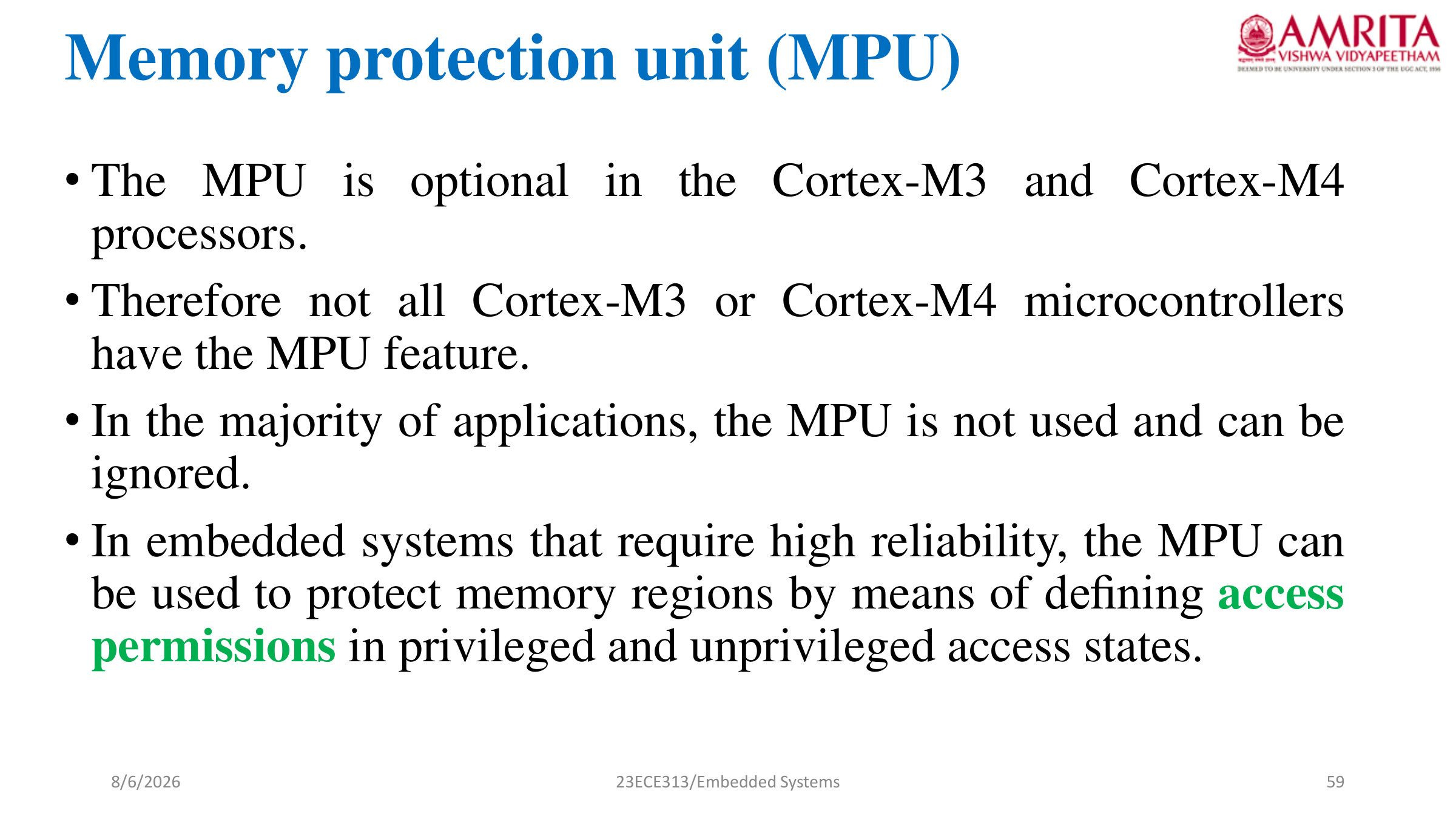
1. MPU Architecture Overview:
The MPU divides the 4 GB memory map into up to 8 programmable regions (numbered 0 to 7). A background region with default privileged access permissions can be enabled via PRIVDEFENA.
2. Key MPU Control Registers:
MPU->CTRL: Enables MPU (ENABLEbit), enables default memory map in privileged mode (PRIVDEFENA), and enables MPU during HardFault and NMI (HFNMIENA).MPU->RNR: Region Number Register (0 to 7) to select active region.MPU->RBAR: Region Base Address Register (must be aligned to region size).MPU->RASR: Region Attribute and Size Register:SIZEbits [5:1]: Region size = 2^(SIZE+1) bytes (minimum 32 bytes).APbits [26:24]: Access Permissions (Privileged RW / User None, Privileged RO / User RO, etc.).XNbit [28]: Execute Never (prevents code execution from data/stack).TEX, C, Bbits: Cache and write buffer memory attributes.SRDbits [15:8]: Sub-Region Disable field.
3. Sub-Region Disable (SRD) Mechanism:
- Any MPU region of size ≥ 256 bytes is automatically split into 8 equal-sized sub-regions.
- The
SRDfield contains 8 bits (one bit for each sub-region). - Writing a
1to bit k disables sub-region k, allowing that slice to fall through to lower priority region rules or the background region. - Exam Benefit: Allows carving out unprivileged memory "holes" without consuming multiple precious MPU region slots!
4. MemManage Fault Violation:
When an instruction fetch or data access violates MPU permissions (or attempts to execute in an XN region), the processor aborts the transaction and triggers a MemManage Fault. The fault address is stored in MMFAR, and status flags are set in MFSR.
2. Assembly Branch Execution & The EPSR Thumb-Bit (T-Bit) Rule: Explain why branching to an even address causes an immediate UsageFault (INVSTATE).
Direct Reference: 1 23ECE313_ES_Ch4 Text 1.pdf (Slides 25, 48)
1. The EPSR T-Bit (Bit 24) Rule:
ARM Cortex-M processors exclusively execute the Thumb-2 instruction set. They do NOT possess a 32-bit ARM instruction decoder state. Therefore, the T-bit (Bit 24) in the EPSR MUST ALWAYS BE 1 during instruction execution.
2. Function Pointers and Indirect Branches (BX / BLX):
In the ARM architecture, when executing an indirect branch via a register (e.g. BX R0, BLX R3, or loading PC via LDR PC, [R1]), Bit 0 of the target address is used by hardware to update the T-bit:
- If Bit 0 of target address =
1──► Sets EPSR T-bit to 1 (Thumb State). Target instruction executed atAddress & ~1. - If Bit 0 of target address =
0──► Attempts to clear EPSR T-bit to 0 (ARM State).
3. Why an Even Address Triggers UsageFault:
// Example: Function resides at Flash address 0x08001000
void (*my_func)(void) = (void (*)(void))0x08001000; // EVEN ADDRESS (Bit 0 = 0)
my_func(); // Executes BX R0 with R0 = 0x08001000
Hardware attempts to switch the CPU into ARM state by clearing the T-bit to 0. Since Cortex-M does not support ARM state, the core detects an illegal state transition and immediately triggers a UsageFault with INVSTATE (Invalid State) bit set in UFSR!
0x08001001 for a function physically located at 0x08001000).
3. Vector Table Offset Register (VTOR) Sizing & Alignment Derivation: Calculate the minimum table size and power-of-2 alignment boundary for an MCU with 32 and 75 external IRQs.
Direct Reference: 2 23ECE313_ES_Ch_Txt1.pdf (Slides 20, 34–37)
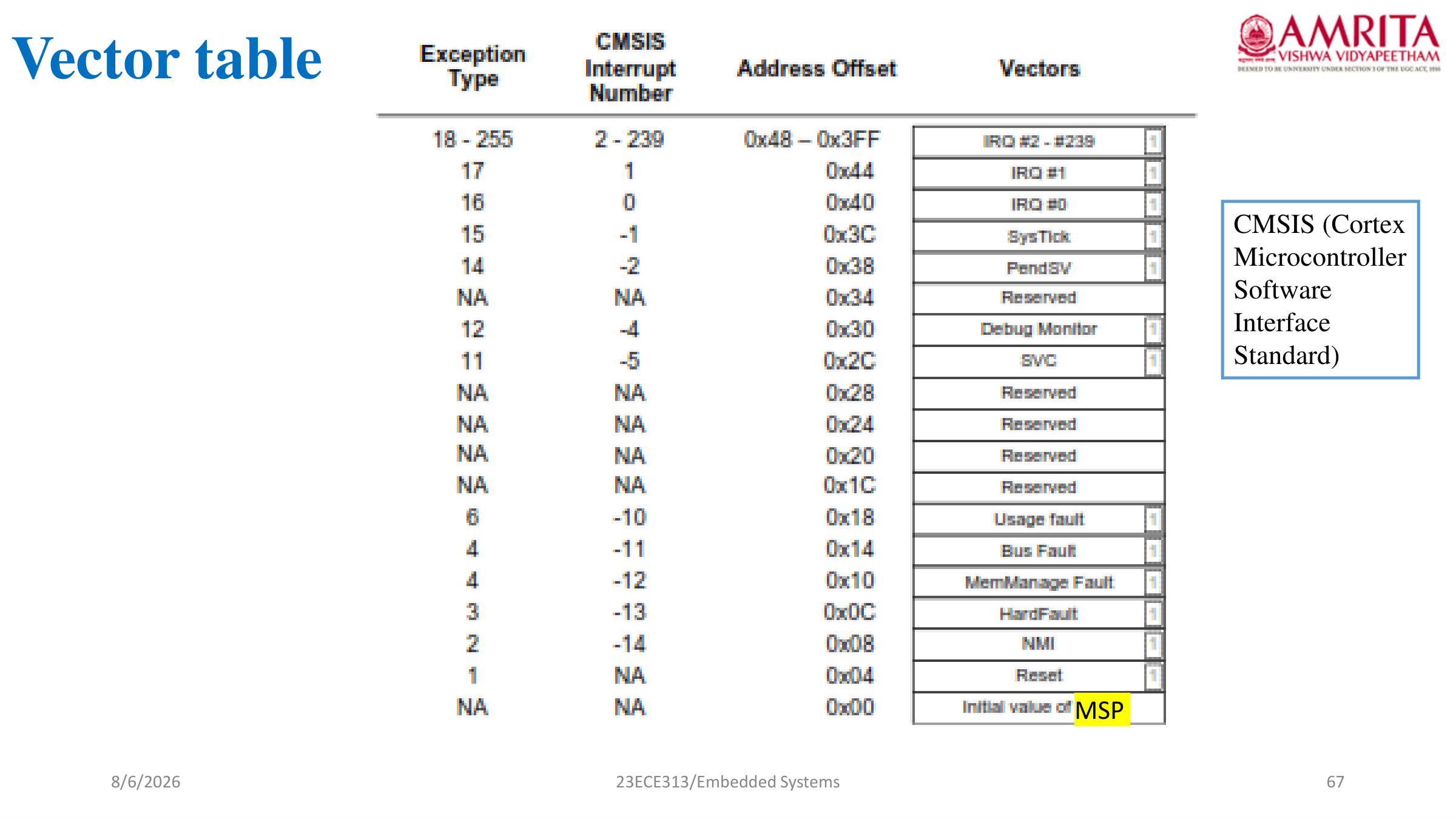
1. Mathematical Formula for Vector Table Size:
Every Cortex-M vector table begins with 16 system exception vectors (Vectors 0 to 15), followed by N external interrupt vectors (IRQ0 to IRQ N-1). Each vector entry is a 32-bit (4-byte) pointer.
Total Vector Table Size = (16 System Exceptions + N External IRQs) × 4 bytes
2. ARMv7-M VTOR Alignment Rule:
The base address programmed into VTOR (Address: 0xE000ED08) must be aligned to a power-of-2 boundary that is greater than or equal to the total table size, with an absolute minimum hardware alignment of 128 bytes (32 words).
3. Calculation for Case A: Microcontroller with 32 External IRQs:
- Total Vector Entries:
16 + 32 = 48 words. - Memory Size:
48 × 4 = 192 bytes. - Required Power-of-2 Alignment: The smallest power of 2 ≥ 192 is 256 bytes (0x100).
- Conclusion: Base address in VTOR must end in
0x00(Bits [7:0] = 0).
4. Calculation for Case B: Microcontroller with 75 External IRQs (e.g. STM32F446RE):
- Total Vector Entries:
16 + 75 = 91 words. - Memory Size:
91 × 4 = 364 bytes. - Required Power-of-2 Alignment: The smallest power of 2 ≥ 364 is 512 bytes (0x200).
- Conclusion: Base address in VTOR must end in a multiple of
0x200(Bits [8:0] = 0).
4. Explain the CoreSight On-Chip Debug Architecture and Contrast the 4 Trace Units: DWT, ITM, ETM, and TPIU.
Direct Reference: 4 23ECE313_ES_Ch14_Txt 1a.pdf (Slides 5–12); 5 23ECE313_ES_Ch15_Txt 1a.pdf (Slides 4–10)
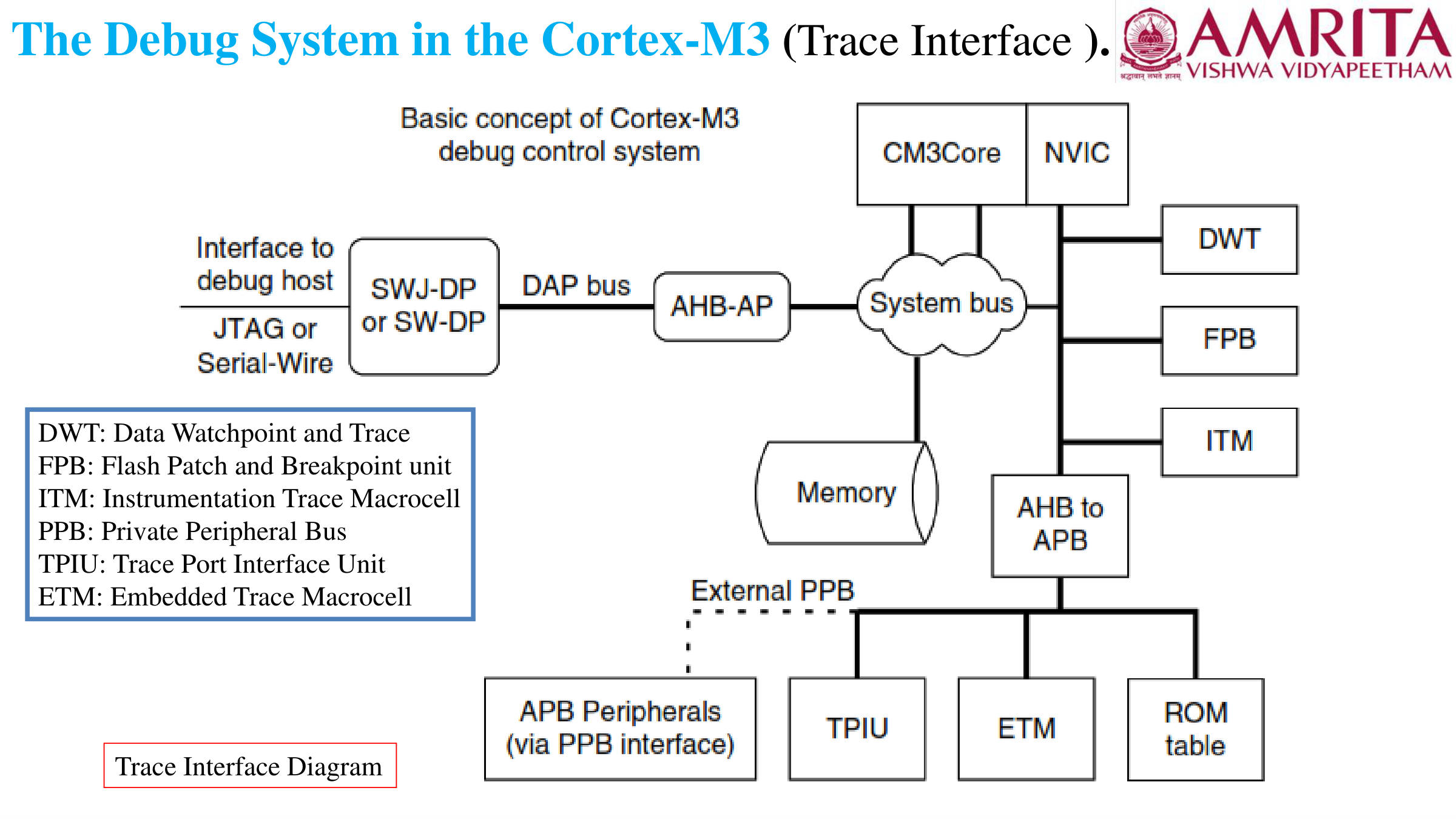
1. Non-Intrusive Tracing vs Intrusive Debugging:
- Intrusive Debugging (Halt Mode): Halts the CPU clock. Breaks hard real-time systems (e.g., motor drive shorts out, CAN bus communication times out).
- Non-Intrusive Trace: CoreSight monitors execution in real-time at full CPU speed without halting the CPU, transmitting trace packets through external pins.
2. Detailed Functions of the Four CoreSight Trace Units:
| Trace Unit | Full Name | Primary Function & Exam Keywords |
|---|---|---|
| DWT | Data Watchpoint and Trace | Contains 4 hardware watchpoint comparators. Monitors data memory accesses (triggering trace on read/write to a specific variable). Measures cycle counts (CYCCNT) for profiling. |
| ITM | Instrumentation Trace Macrocell | Enables high-speed software printf debugging without UART hardware. Application writes directly to ITM stimulus registers (e.g. ITM->PORT[0]), which outputs data over the 1-pin SWO (Serial Wire Output) line. |
| ETM | Embedded Trace Macrocell | Reconstructs the exact instruction execution history in real time. Captures every branch taken/not-taken and exception entry to provide full instruction trace back in time. |
| TPIU | Trace Port Interface Unit | Acts as a hardware multiplexer and serializer. Formats and combines data streams from ITM and ETM, outputting them to external debug hardware (e.g. Keil ULINKpro, Segger J-Trace) via SWO or multi-pin Trace Port. |
5. Draw and explain the Cortex-M Bus Architecture (I-Code, D-Code, and System Bus) and the AHB-Lite Bus Matrix.
Direct Reference: 1 23ECE313_ES_Ch4 Text 1.pdf (Slides 14–15)
1. The Three Primary AHB-Lite Buses:
- I-Code Bus (Instruction Fetch): 32-bit AHB-Lite bus dedicated to fetching instructions from the Code space (
0x00000000 - 0x1FFFFFFF), primarily Flash/ROM. - D-Code Bus (Data Fetch from Code Space): 32-bit AHB-Lite bus used to fetch literal pools, constants, and table data stored within the Code space (
0x00000000 - 0x1FFFFFFF). - System Bus (S-Bus): 32-bit AHB-Lite bus used for all data accesses to SRAM (
0x20000000), Peripherals (0x40000000), and External Memories (0x60000000). Can also fetch instructions from SRAM.
2. The Multi-Layer AHB Bus Matrix Advantage:
Cortex-M uses a Harvard architecture enabled by a multi-layer AHB matrix. Because instruction fetches (on I-Code) and data accesses (on System Bus or D-Code) travel over independent physical buses simultaneously, the processor can fetch an instruction and perform a data load/store in the exact same clock cycle without bus contention!
3. The APB (Advanced Peripheral Bus) Bridge:
Connects the high-speed AHB system bus to lower-power peripherals (USART, SPI, I2C, Timers, ADC). The APB bridge translates AHB burst transfers into simplified APB read/write cycles and operates at lower clock frequencies to save power.
6. Explain the Three Reset Types in Cortex-M and Self-Reset Control using the AIRCR Register (VECTKEY and SYSRESETREQ).
Direct Reference: 1 23ECE313_ES_Ch4 Text 1.pdf (Slide 75); 3 23ECE313_ES_Ch12_Txt1.pdf (Slide 44)
1. Three Reset Types in Cortex-M Architecture:
- Power-on Reset (POR): Cold reset initiated when power is first applied. Resets the entire microcontroller: processor core, system control logic, all peripherals, and debug blocks.
- System Reset: Warm reset initiated by the external reset pin (
NRST), independent watchdog timer, or software command (SYSRESETREQ). Resets processor core and all peripherals, but preserves debug logic so active debug sessions are not dropped. - Processor Reset: Resets only the processor core (internal registers, pipeline, and NVIC). Peripherals and bus bridges continue active operation. Driven by debuggers via
VECTRESET.
2. Self-Reset Control via AIRCR (Address: 0xE000ED0C):
The Application Interrupt and Reset Control Register allows software to trigger a clean system reboot:
3. The VECTKEY Security Protection:
To prevent accidental system resets caused by errant software or stack corruption, writes to AIRCR MUST write the secret unlock key 0x05FA into bits [31:16] (VECTKEY field). If any other value is written, the entire write is rejected by hardware!
4. CMSIS Register Implementation:
void System_SelfReset(void) {
    __DSB(); // Ensure all outstanding memory transactions finish
    SCB->AIRCR = (0x05FA << SCB_AIRCR_VECTKEY_Pos) | SCB_AIRCR_SYSRESETREQ_Msk;
    __DSB(); // Wait for reset to assert
    while (1); // Trap until hardware reset executes
}
7. Compare Low-Power Modes (Sleep, Deep Sleep, Standby), SCR Register Control Bits, and the Wakeup Interrupt Controller (WIC).
Direct Reference: 3 23ECE313_ES_Ch12_Txt1.pdf (Slides 38–42)
| Mode | Core Clock | Peripherals & Clocks | Voltage Regulator | Wakeup Sources & Latency |
|---|---|---|---|---|
| Sleep Mode | Gated (Off) | Running (HSI, HSE, PLL, Timers active) | Main Regulator ON | Any interrupt. Fast wakeup (< 10 cycles). |
| Deep Sleep (Stop) | Gated (Off) | High-speed clocks stopped. SRAM and register contents retained. | Low-power regulator mode | EXTI, RTC alarm, WIC. Medium wakeup (~few microseconds). |
| Standby Mode | Off | Entire core domain powered down. SRAM lost! Only Backup Domain active. | Regulator Powered Down | Wakeup pin (WKUP), RTC alarm, NRST. Cold boot reset sequence. |
1. SCR (System Control Register - Address: 0xE000ED10) Control Bits:
- Bit 1 (SLEEPONEXIT): When set to 1, processor automatically enters sleep mode immediately upon exiting the lowest-priority ISR, without executing thread background code. Perfect for purely interrupt-driven sensor nodes!
- Bit 2 (SLEEPDEEP):
0= Enter standard Sleep mode onWFI;1= Enter Deep Sleep / Stop mode onWFI. - Bit 4 (SEVONPEND): If 1, even disabled/masked pending interrupts generate an event to wake processor from
WFE.
2. Wakeup Interrupt Controller (WIC):
In Deep Sleep mode, the main core power domain and NVIC clocks are shut down to achieve microamp currents. The WIC is a small, ultra-low-power shadow controller that stays powered. When an external line asserts an interrupt, the WIC signals the Power Management Unit to wake the main voltage regulator, restore clocks, and hand off the pending interrupt directly to the NVIC!
8. Write a CMSIS Register C Function to generate a millisecond hardware delay using the SysTick Timer (16 MHz clock) without interrupts.
Direct Reference: 3 23ECE313_ES_Ch12_Txt1.pdf (Slides 35–37); lab/systick.c
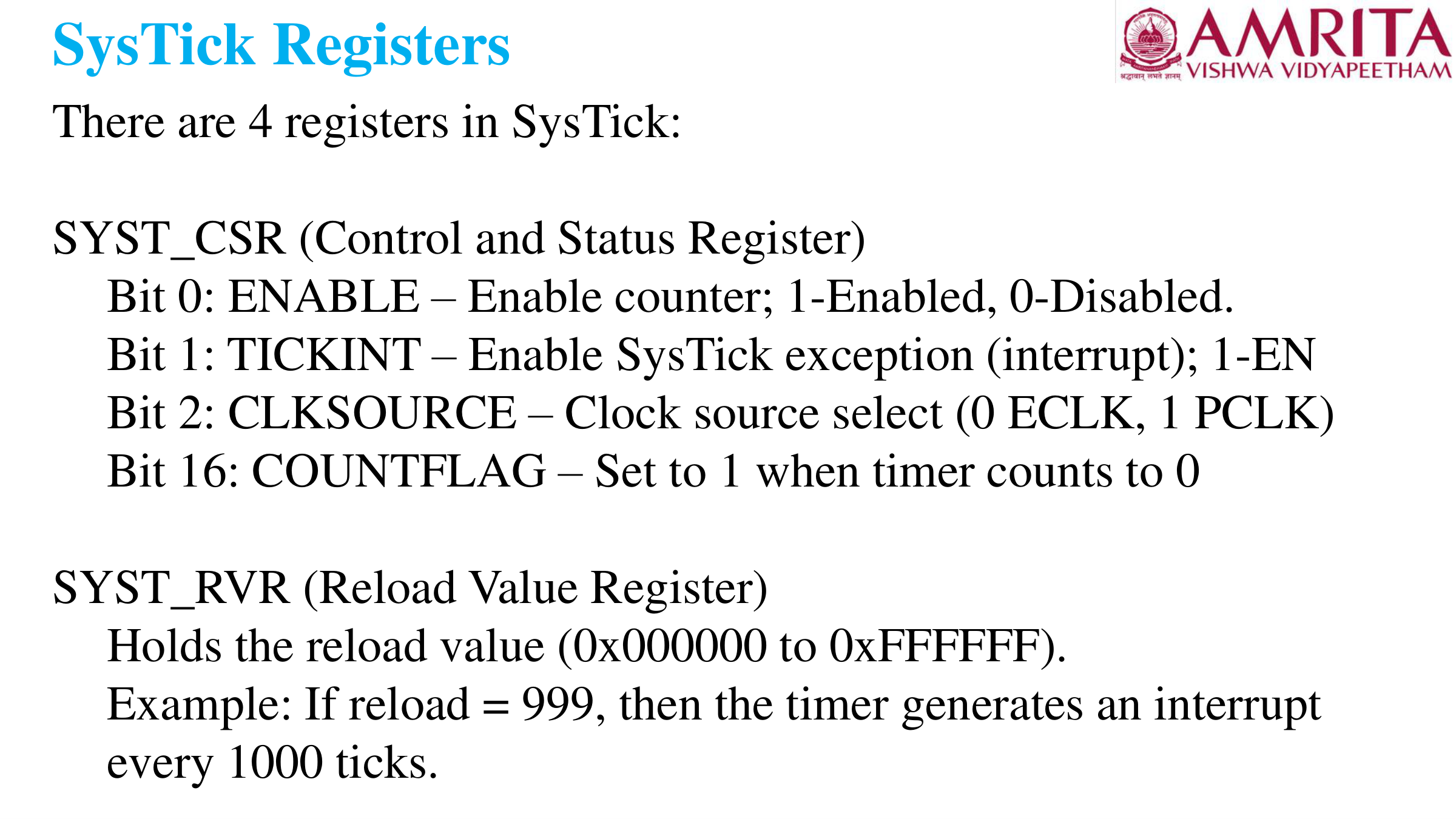
1. Mathematical Derivation for 1 Millisecond Delay:
- Processor Clock:
f_CPU = 16 MHz = 16,000,000 Hz - Time for 1 millisecond:
T = 1 ms = 0.001 s - Number of clock cycles required:
N = 16,000,000 × 0.001 = 16,000 cycles - Since counter counts from
LOADdown to 0 (a total ofLOAD + 1states): SysTick->LOAD = 16,000 - 1 = 15,999 (0x3E7F)
2. Complete CMSIS Register Implementation:
#include "stm32f4xx.h"

void SysTick_Delay_ms(uint32_t ms) {
    // 1. Disable SysTick during configuration
    SysTick->CTRL = 0;

    // 2. Load count value for 1 ms (16,000 cycles at 16 MHz)
    SysTick->LOAD = 15999;

    // 3. Clear current value register and clear COUNTFLAG
    SysTick->VAL = 0;

    // 4. Enable SysTick with Processor Clock (Bit 2: CLKSOURCE = 1, Bit 0: ENABLE = 1)
    // No interrupt enable (TICKINT = 0)
    SysTick->CTRL = SysTick_CTRL_CLKSOURCE_Msk | SysTick_CTRL_ENABLE_Msk;

    // 5. Loop for the requested number of milliseconds
    for (uint32_t i = 0; i < ms; i++) {
        // Wait until COUNTFLAG (Bit 16) is set to 1 by hardware
        while (!(SysTick->CTRL & SysTick_CTRL_COUNTFLAG_Msk));
    }

    // 6. Disable SysTick after delay finishes
    SysTick->CTRL = 0;
}

int main(void) {
    // Enable GPIOA clock and configure PA5 as output
    RCC->AHB1ENR |= RCC_AHB1ENR_GPIOAEN;
    GPIOA->MODER &= ~(3U << (5 * 2));
    GPIOA->MODER |=  (1U << (5 * 2));

    while (1) {
        GPIOA->ODR ^= (1U << 5);      // Toggle PA5 LED
        SysTick_Delay_ms(500);        // Accurate 500 ms delay
    }
}
9. Complete Peripheral Integration: Interfacing PC13 Pushbutton (EXTI13), PA0 Analog Sensor (ADC1), and PA5 PWM LED (TIM2_CH1). Write C code where button press updates LED brightness.
Direct Reference: 7 23ECE313_ES_ Mazidi.pdf & STM32F446RE_Timers_PWM_ADC_Mazidi.pdf
1. Complete Multi-Peripheral Circuit Diagram:
2. System Architecture & Operation Flow:
- Standby State: System operates in low-power sleep (
__WFI()) while TIM2 continuously outputs PWM on PA5. - Interrupt Event: User presses PC13 button, asserting falling edge on EXTI13.
- ISR Execution (
EXTI15_10_IRQHandler):- Trigger software conversion on ADC1 (
SWSTART). - Poll until
EOCflag is set inADC1->SR. - Read 12-bit ADC result (0 to 4095).
- Scale and write the ADC result directly to
TIM2->CCR1. - Clear pending bit by writing 1:
EXTI->PR = (1U << 13);.
- Trigger software conversion on ADC1 (
3. Complete Embedded C Program:
#include "stm32f4xx.h"

void System_Peripherals_Init(void) {
    // 1. Enable Peripheral Clocks
    RCC->AHB1ENR |= RCC_AHB1ENR_GPIOAEN | RCC_AHB1ENR_GPIOCEN; // GPIOA & GPIOC
    RCC->APB2ENR |= RCC_APB2ENR_SYSCFGEN | RCC_APB2ENR_ADC1EN; // SYSCFG & ADC1
    RCC->APB1ENR |= RCC_APB1ENR_TIM2EN;                        // TIM2

    // 2. Configure PC13 as Digital Input with Pull-Up (Pushbutton)
    GPIOC->MODER &= ~(3U << (13 * 2)); // Input mode ('00')
    GPIOC->PUPDR &= ~(3U << (13 * 2));
    GPIOC->PUPDR |=  (1U << (13 * 2)); // Pull-Up ('01')

    // 3. Configure PA0 as Analog Mode (ADC1_IN0)
    GPIOA->MODER |= (3U << (0 * 2));   // Analog mode ('11')

    // 4. Configure PA5 as Alternate Function AF1 (TIM2_CH1 PWM)
    GPIOA->MODER &= ~(3U << (5 * 2));
    GPIOA->MODER |=  (2U << (5 * 2));  // Alternate function ('10')
    GPIOA->AFR[0] &= ~(0xFU << (5 * 4));
    GPIOA->AFR[0] |=  (1U   << (5 * 4)); // AF1 = TIM2_CH1

    // 5. Configure EXTI13 for PC13
    SYSCFG->EXTICR[3] &= ~(0xFU << 4);
    SYSCFG->EXTICR[3] |=  (2U   << 4); // Port C = 0x2
    EXTI->FTSR |= (1U << 13);          // Falling trigger
    EXTI->IMR  |= (1U << 13);          // Unmask interrupt line 13

    NVIC_SetPriority(EXTI15_10_IRQn, 2);
    NVIC_EnableIRQ(EXTI15_10_IRQn);

    // 6. Configure ADC1 (Channel 0, PA0)
    ADC1->SMPR2 |= (4U << 0);          // 84 cycles sample time
    ADC1->SQR1 = 0;                    // 1 conversion
    ADC1->SQR3 = 0;                    // Channel 0
    ADC1->CR2 |= ADC_CR2_ADON;         // Turn on ADC

    // 7. Configure TIM2 for 1 kHz PWM with 12-bit range (ARR = 4095)
    TIM2->PSC = 3;                     // 16 MHz / 4 = 4 MHz timer clock
    TIM2->ARR = 4095;                  // Matches 12-bit ADC resolution!
    TIM2->CCR1 = 2048;                 // Initial 50% duty cycle
    TIM2->CCMR1 |= (6U << 4) | TIM_CCMR1_OC1PE; // PWM Mode 1
    TIM2->CCER  |= TIM_CCER_CC1E;      // Enable channel 1 output
    TIM2->CR1   |= TIM_CR1_CEN;        // Start counter
}

// EXTI15_10 Interrupt Handler for Button Press
void EXTI15_10_IRQHandler(void) {
    if (EXTI->PR & (1U << 13)) {
        // Start ADC conversion on PA0
        ADC1->CR2 |= ADC_CR2_SWSTART;
        while (!(ADC1->SR & ADC_SR_EOC)); // Wait for conversion

        uint16_t adc_val = ADC1->DR;      // Read 12-bit analog value (0-4095)

        // Dynamically update PWM duty cycle (matches ARR = 4095)
        TIM2->CCR1 = adc_val;

        // Clear interrupt pending bit (WRITE 1 TO CLEAR)
        EXTI->PR = (1U << 13);
    }
}

int main(void) {
    System_Peripherals_Init();

    while (1) {
        __WFI(); // Sleep until button press interrupt arrives
    }
}
📝 Practice Question Paper - Set 4 (50 Marks)
Model Exam Set 4: TM4C123 & Fault MasteryDedicated coverage of TM4C123 (Tiva C Series) Architecture, Register-Level Peripheral Programming, and In-Depth Fault Diagnosis. Click any question to reveal complete step-by-step solutions:
1. Explain the TM4C123 (Tiva C) Microcontroller Architecture, Bus Interconnects, and the System Control Run-Mode Clock Gating (RCGC) Registers.
Direct Reference: 7 23ECE313_ES_ Mazidi.pdf (Chapter 1 & 2) / TM4C123GH6PM Datasheet
1. Core Architecture Overview:
- Processor Core: ARM Cortex-M4F operating at up to 80 MHz, with 32-bit Harvard architecture, single-precision Hardware Floating Point Unit (FPU), and Thumb-2 ISA.
- On-Chip Memory: 256 KB Flash memory, 32 KB SRAM, 2 KB EEPROM, and dedicated ROM containing TivaWare peripheral driver library.
- Bus Interconnect: Multi-layer Advanced Microcontroller Bus Architecture (AMBA) featuring high-speed AHB (Advanced High-Performance Bus) for Flash/SRAM and APB (Advanced Peripheral Bus) for legacy peripherals. Certain ports (Port A-F) can be software-configured to operate on either APB or advanced AHB for higher throughput.
2. Run-Mode Clock Gating Control (RCGC) System:
In TM4C123, all peripherals are powered down by default to conserve energy. Before accessing any peripheral register, software must explicitly gate the clock using the System Control Block (Base: 0x400FE000):
SYSCTL_RCGCGPIO_R(Offset0x608): Clock gating for GPIO Ports A through F (Bit 0 = Port A, Bit 1 = Port B, ..., Bit 5 = Port F).SYSCTL_RCGCTIMER_R(Offset0x604): Clock gating for 16/32-bit General Purpose Timer Modules (Timer 0 to Timer 5).SYSCTL_RCGCADC_R(Offset0x638): Clock gating for ADC Modules (Bit 0 = ADC0, Bit 1 = ADC1).SYSCTL_RCGCPWM_R(Offset0x640): Clock gating for PWM Modules 0 and 1.
volatile uint32_t delay = SYSCTL_RCGCGPIO_R;) before touching any peripheral register, or the CPU will trigger an immediate BusFault!
2. Explain the TM4C123 GPIO Architecture and the Hardware Address-Bit Masking Mechanism in the GPIODATA Register.
Direct Reference: 7 23ECE313_ES_ Mazidi.pdf (Chapter 2, Section 2.3)
1. Why Address-Bit Masking is Needed:
Traditional microcontrollers require software read-modify-write sequences (PORT |= (1<<2)) to modify individual I/O pins, which creates severe race conditions when interrupts fire between the read and write. TM4C123 eliminates this by mapping address bus bits [9:2] directly as an 8-bit pin mask!
2. How the Address Mask Works:
- Every GPIO port occupies a 1 KB address space for its data register (from offset
0x000to0x3FC). - The base address is
0x40025000for Port F. Bits [9:2] of the address offset determine which of the 8 pins (PF7–PF0) can be read or written. - If address bit
(2 + n)is1, then pin n is affected by the read/write. If bit(2 + n)is0, pin n is hardware-protected and remains unmodified!
To access ONLY Pin 1, Pin 2, and Pin 3 of Port F (RGB LED):
• Pin mask: Bit 1 (1<<1 = 0x02) | Bit 2 (1<<2 = 0x04) | Bit 3 (1<<3 = 0x08) =
0x0E (0b00001110)• Shift left by 2 to align with address bits [9:2]:
0x0E << 2 = 0x38• Masked Address:
0x40025000 + 0x38 = 0x40025038• Writing
GPIO_PORTF_DATA_BITS_R[0x0E] = 0x04; turns on ONLY the Blue LED (Pin 2) without modifying any other pin!
3. Key TM4C123 GPIO Configuration Registers:
GPIODIR: 0 = Input, 1 = Output.GPIODEN: Digital Enable (1 = Digital I/O enabled; 0 = Disabled for analog mode).GPIOPUR/GPIOPDR: Internal Pull-Up / Pull-Down resistor enable.GPIOLOCK&GPIOCR: Used to unlock special pins (e.g., PF0 and PD7 which default to NMI/JTAG). Write0x4C4F434BtoGPIOLOCK, then set commit registerGPIOCRto0xFF.
3. Explain the TM4C123 On-Chip ADC Architecture, the 4 Sample Sequencers (SS0–SS3), and the Sequence Control Register (SSCTL).
Direct Reference: 7 23ECE313_ES_ Mazidi.pdf (Chapter 8, ADC Programming)
1. ADC Core Specifications:
TM4C123 features two independent 12-bit Successive Approximation ADC modules (ADC0 and ADC1) with up to 12 shared analog input channels (AIN0 to AIN11) and sample rates up to 1 MSPS.
2. The Four Sample Sequencers:
| Sequencer | FIFO Depth | Max Samples per Trigger | Typical Use Case |
|---|---|---|---|
| SS0 | 8 samples | 8 | Complex multi-sensor acquisition / sensor fusion |
| SS1 | 4 samples | 4 | Medium multichannel telemetry |
| SS2 | 4 samples | 4 | Multichannel acquisition with oversampling |
| SS3 | 1 sample | 1 | Single-channel conversion (e.g. potentiometer / temperature sensor) |
3. Key ADC Registers & Configuration Steps:
ADC0_ACTSS_R: Active Sample Sequencer. Clear bit 3 to disable SS3 during configuration, then set bit 3 to enable it afterwards.ADC0_EMUX_R: Event Multiplexer Select. Writing0x0000configures software trigger (Processor trigger) for SS3.ADC0_SSMUX3_R: Sample Sequencer 3 Input Multiplexer. Write channel number (e.g.0forAIN0on PE3).ADC0_SSCTL3_R: Sample Sequencer 3 Control. Set bit 1 (END0) to mark it as the last sample, and bit 2 (IE0) to assert raw interrupt flag when conversion completes (Write0x0006).ADC0_PSSI_R: Processor Sample Initiate. Write0x0008to start SS3 conversion by software.ADC0_RIS_R: Raw Interrupt Status. Poll Bit 3 to wait for conversion completion.ADC0_SSFIFO3_R: Read 12-bit result (0 to 4095).
4. Methods of Dealing with Faults: Explain the Configurable Fault Status Register (CFSR = MMFSR + BFSR + UFSR) and Fault Escalation.
Direct Reference: 3 23ECE313_ES_Ch12_Txt1.pdf (Slides 16–22)
1. Structure of the CFSR Register (Address: 0xE000ED28):
The 32-bit CFSR register is physically partitioned into three sub-registers:
Bit:  [31 ------------- 16] [15 -------------- 8] [7 ---------------- 0]
      |        UFSR        |        BFSR        |        MMFSR         |
| (Usage Fault Stat) | (Bus Fault Status) | (MemManage Status) |- MMFSR (Bits [7:0] - MemManage Fault Status):
IACCVIOL(Bit 0): Instruction access violation (e.g. attempted execution from an XN region).DACCVIOL(Bit 1): Data access violation (e.g. unprivileged write to privileged region).MMARVALID(Bit 7): MemManage Fault Address Register (MMFAR) holds valid fault address.
- BFSR (Bits [15:8] - Bus Fault Status):
IBUSERR(Bit 8): Instruction bus error during fetch.PRECISERR(Bit 9): Precise data bus error (stacked PC is exact;BFARis valid).IMPRECISERR(Bit 10): Imprecise data bus error from Write Buffer (stacked PC is delayed;BFARinvalid!).BFARVALID(Bit 15): Bus Fault Address Register (BFAR) contains valid fault address.
- UFSR (Bits [31:16] - Usage Fault Status):
UNDEFINSTR(Bit 16): Attempted execution of undefined/illegal opcode.INVSTATE(Bit 17): Illegal state transition (EPSR T-bit cleared to 0 by branch to even address).INVPC(Bit 18): Invalid PC load from illegal EXC_RETURN.UNALIGNED(Bit 24): Unaligned memory access (if trap enabled in CCR).DIVBYZERO(Bit 25): Divide-by-zero executed (if trap enabled in CCR).
2. Fault Escalation to HardFault:
If a configurable fault occurs while its handler is disabled in SHCSR (System Handler Control and State Register), or if a fault occurs inside an existing fault handler of equal or higher priority, the processor escalates the exception to a HardFault. In HFSR, the FORCED bit (Bit 30) is set to indicate escalation!
5. Write an Assembly Trampoline and C HardFault Handler to extract the stacked PC, LR, xPSR, and diagnose fault causes.
Direct Reference: 3 23ECE313_ES_Ch12_Txt1.pdf (Slides 23–25)
1. Step 1: Assembly Trampoline (Determines MSP vs PSP):
__asm void HardFault_Handler(void) {
    TST LR, #4          // Test Bit 2 of EXC_RETURN (0 = MSP was used, 1 = PSP was used)
    ITE EQ
    MRSEQ R0, MSP       // Stack pointer was MSP -> pass to C handler in R0
    MRSNE R0, PSP       // Stack pointer was PSP -> pass to C handler in R0
    B HardFault_Handler_C // Branch to C diagnostic function
}
2. Step 2: C Diagnostic Handler Function:
void HardFault_Handler_C(uint32_t *stack_frame) {
    // Extract hardware stacked registers from stack pointer
    uint32_t stacked_r0  = stack_frame[0];
    uint32_t stacked_r1  = stack_frame[1];
    uint32_t stacked_r2  = stack_frame[2];
    uint32_t stacked_r3  = stack_frame[3];
    uint32_t stacked_r12 = stack_frame[4];
    uint32_t stacked_lr  = stack_frame[5];
    uint32_t stacked_pc  = stack_frame[6]; // FAULTING INSTRUCTION ADDRESS!
    uint32_t stacked_psr = stack_frame[7];

    // Read System Control Block Fault Status Registers
    uint32_t cfsr = SCB->CFSR; // Configurable Fault Status
    uint32_t hfsr = SCB->HFSR; // HardFault Status
    uint32_t bfar = SCB->BFAR; // Bus Fault Address (if BFARVALID is set)
    uint32_t mmfar = SCB->MMFAR; // MemManage Fault Address (if MMARVALID is set)

    // Check if HardFault was forced by an unhandled configurable fault
    if (hfsr & (1U << 30)) {
        // FORCED bit set: Escalated from BusFault, MemManage, or UsageFault
    }

    // Hang or initiate safe system reset
    __disable_irq();
    while (1); // Trap debugger here to inspect registers
}
6. Explain the Lockup State in Cortex-M processors: Root causes, hardware response, and recovery procedures.
Direct Reference: 3 23ECE313_ES_Ch12_Txt1.pdf (Slide 26)
1. Definition of Lockup:
The Lockup state is a terminal fault condition in the ARM Cortex-M core that occurs when an exception/fault is triggered while the processor is already executing inside the HardFault Handler or NMI Handler (known as a Double Fault or recursive fault).
2. Primary Root Causes:
- Corrupted Stack Pointer: The stack pointer points to invalid memory or unmapped RAM. When HardFault attempts to push registers to the stack, a BusFault occurs, which cannot be serviced because HardFault is already active!
- Corrupted Vector Table: The vector table entry for
HardFault_HandlerorNMI_Handlerpoints to invalid memory or has its LSB cleared to 0 (violating Thumb state). - Bus Error during Vector Fetch at Reset: Address
0x00000000or0x00000004returns a bus error during boot.
3. Hardware Response during Lockup:
- The processor halts all instruction fetching and execution immediately.
- The core asserts the external hardware output signal
LOCKUP. - In silicon implementations (like STM32 and TM4C), the
LOCKUPsignal can be wired directly to an internal Watchdog Timer or System Reset Controller to force an automatic warm reboot.
4. Recovery:
Lockup cannot be exited by software or regular interrupts. Recovery is only possible via a hardware Power-on Reset (POR), External Reset pin assertion (NRST), or a Watchdog Timer Reset.
7. Explain the TM4C123 External GPIO Interrupt Configuration Registers (GPIOIS, GPIOIBE, GPIOIEV, GPIOIM, and GPIOICR).
Direct Reference: 7 23ECE313_ES_ Mazidi.pdf (Chapter 6, Interrupts)
1. Five-Stage Register Pipeline for GPIO Interrupts:
| Register | Name | Function & Bit Values |
|---|---|---|
GPIOIS |
Interrupt Sense | 0 = Edge-sensitive interrupt.1 = Level-sensitive interrupt. |
GPIOIBE |
Interrupt Both Edges | 0 = Interrupt generation controlled by GPIOIEV.1 = Both rising and falling edges trigger an interrupt. |
GPIOIEV |
Interrupt Event | 0 = Falling edge (or Low level).1 = Rising edge (or High level). |
GPIOIM |
Interrupt Mask | 0 = Interrupt masked (disabled from reaching NVIC).1 = Interrupt unmasked (sent to NVIC). |
GPIOICR |
Interrupt Clear | Write 1 to Clear: Software MUST write a 1 to the corresponding bit in GPIOICR inside the ISR to acknowledge and clear the interrupt flag! Writing 0 has no effect. |
2. Status Registers:
GPIORIS(Raw Interrupt Status): Shows if an interrupt condition occurred on the pin, regardless of mask.GPIOMIS(Masked Interrupt Status): Shows if an active interrupt is currently sent to the NVIC (RIS AND IM).
8. C Program for TM4C123: Configure Port F Pin 4 (SW1 Pushbutton) with internal pull-up and Pin 2 (Blue LED) with toggling logic.
Direct Reference: 7 23ECE313_ES_ Mazidi.pdf (Chapter 2 & 3)
1. Hardware Interfacing & Port F Pin Map:
- PF4: On-board Pushbutton SW1 (Active-Low: Pressed = 0, Released = 1). Requires internal pull-up!
- PF2: On-board Blue LED (Active-High: 1 = ON, 0 = OFF).
2. Complete C Program:
#include
#include "tm4c123gh6pm.h"

void PortF_Init(void) {
    // 1. Enable Clock for Port F in RCGCGPIO (Bit 5 = 1)
    SYSCTL_RCGCGPIO_R |= 0x20;

    // 2. Wait for clock to stabilize (3 cycles)
    volatile uint32_t delay = SYSCTL_RCGCGPIO_R;

    // 3. Unlock Port F commit register (Required for PF0, good practice)
    GPIO_PORTF_LOCK_R = 0x4C4F434B; // Secret unlock key
    GPIO_PORTF_CR_R |= 0x14;        // Commit PF4 and PF2

    // 4. Configure Directions: PF4 is Input (0), PF2 is Output (1)
    GPIO_PORTF_DIR_R &= ~0x10;      // Clear bit 4 (PF4 Input)
    GPIO_PORTF_DIR_R |=  0x04;      // Set bit 2 (PF2 Output)

    // 5. Disable Analog Mode
    GPIO_PORTF_AMSEL_R &= ~0x14;

    // 6. Disable Alternate Functions (Regular GPIO)
    GPIO_PORTF_AFSEL_R &= ~0x14;

    // 7. Enable Internal Pull-Up Resistor on PF4 (Active-Low button)
    GPIO_PORTF_PUR_R |= 0x10;

    // 8. Enable Digital Functionality on PF4 and PF2
    GPIO_PORTF_DEN_R |= 0x14;
}

int main(void) {
    PortF_Init();

    while (1) {
        // Read PF4: If button is pressed (PF4 reads 0)
        if ((GPIO_PORTF_DATA_R & 0x10) == 0) {
            GPIO_PORTF_DATA_R |= 0x04;  // Turn ON Blue LED
        } else {
            GPIO_PORTF_DATA_R &= ~0x04; // Turn OFF Blue LED
        }
    }
}
9. Comprehensive TM4C123 System Design: Interface Analog Sensor on PE3 (ADC0 SS3), drive DC Motor PWM on PB6 (M0PWM0), with schematic and complete C code.
Direct Reference: 7 23ECE313_ES_ Mazidi.pdf (Chapters 8 & 11)
1. Complete Circuit Schematic:
2. Operational Logic & Calculations:
- ADC0 SS3: Configured for single-sample conversion on Channel 0 (PE3 / AIN0). 12-bit output =
0 to 4095. - PWM Module 0 (PB6): Uses PWM Generator 0. Clock source = 16 MHz System Clock / 64 (PWMDIV) = 250 kHz.
- Period Load Value =
LOAD = 250 - 1 = 249(gives 1 kHz PWM). - Compare Value:
CMPA = (ADC_Value × 249) / 4095(Dynamically varies motor speed from 0% to 100%).
3. Complete C Program:
#include
#include "tm4c123gh6pm.h"

void ADC0_SS3_Init(void) {
    // 1. Enable Clocks for ADC0 and Port E
    SYSCTL_RCGCADC_R |= 0x01;
    SYSCTL_RCGCGPIO_R |= 0x10; // Port E
    volatile uint32_t delay = SYSCTL_RCGCGPIO_R;

    // 2. Configure PE3 as Analog Input (AIN0)
    GPIO_PORTE_DIR_R &= ~0x08;   // Input
    GPIO_PORTE_AFSEL_R |= 0x08;  // Enable Alternate Function
    GPIO_PORTE_DEN_R &= ~0x08;   // Disable Digital
    GPIO_PORTE_AMSEL_R |= 0x08;  // Enable Analog Mode

    // 3. Configure Sample Sequencer 3
    ADC0_ACTSS_R &= ~0x08;       // Disable SS3 during setup
    ADC0_EMUX_R &= ~0xF000;      // Software trigger for SS3
    ADC0_SSMUX3_R = 0;           // Select Channel 0 (AIN0)
    ADC0_SSCTL3_R = 0x0006;      // Set IE0 and END0 (Bit 2 & Bit 1)
    ADC0_ACTSS_R |= 0x08;        // Enable SS3
}

uint16_t ADC0_Read(void) {
    ADC0_PSSI_R = 0x08;                 // Start SS3 conversion
    while ((ADC0_RIS_R & 0x08) == 0);   // Wait for conversion completion
    uint16_t result = ADC0_SSFIFO3_R;   // Read 12-bit value
    ADC0_ISC_R = 0x08;                  // Clear completion flag
    return result;
}

void PWM0_PB6_Init(void) {
    // 1. Enable Clocks for PWM0 and Port B
    SYSCTL_RCGCPWM_R |= 0x01;
    SYSCTL_RCGCGPIO_R |= 0x02; // Port B
    volatile uint32_t delay = SYSCTL_RCGCGPIO_R;

    // 2. Configure PB6 as Alternate Function M0PWM0
    GPIO_PORTB_AFSEL_R |= 0x40;
    GPIO_PORTB_PCTL_R &= ~0x0F000000;
    GPIO_PORTB_PCTL_R |=  0x04000000; // AF4 = PWM
    GPIO_PORTB_DEN_R   |= 0x40;

    // 3. Configure PWM Clock Divider (System Clock / 64)
    SYSCTL_RCC_R |= (1 << 20);        // Enable PWMDIV
    SYSCTL_RCC_R &= ~0x000E0000;      // Clear divider bits
    SYSCTL_RCC_R |=  0x00060000;      // Divide by 64 (250 kHz clock)

    // 4. Configure PWM Generator 0
    PWM0_0_CTL_R = 0;                 // Down-count mode
    PWM0_0_LOAD_R = 249;              // 250 kHz / 250 = 1 kHz PWM
    PWM0_0_CMPA_R = 125;              // Initial 50% duty cycle
    PWM0_0_GENA_R = 0x8C;             // High on LOAD, Low on CMPA
    PWM0_0_CTL_R |= 0x01;             // Enable Generator 0

    // 5. Enable PWM Output on PB6
    PWM0_ENABLE_R |= 0x01;
}

int main(void) {
    ADC0_SS3_Init();
    PWM0_PB6_Init();

    while (1) {
        uint16_t sensor_val = ADC0_Read(); // Read 0 to 4095

        // Scale 12-bit ADC value to PWM LOAD (0 to 249)
        uint32_t pwm_duty = (sensor_val * 249) / 4095;
        if (pwm_duty == 0) pwm_duty = 1; // Prevent underflow

        PWM0_0_CMPA_R = pwm_duty;        // Dynamically adjust motor speed
    }
}
📝 Practice Question Paper - Set 5 (50 Marks)
Model Exam Set 5: FreeRTOS & Memory SystemsIn-Depth Coverage of FreeRTOS Real-Time Kernel, Task Management, Synchronization (Semaphores & Queues), and Advanced Memory Attributes:
1. Draw and explain the FreeRTOS Task State Transition Diagram (Running, Ready, Blocked, Suspended) and the scheduling events that cause transitions.
Direct Reference: lab/Exp 5 and 6.pdf / FreeRTOS Kernel Reference (Chapter 3)
1. Task State Diagram:
               ┌───────────────┐
               │   SUSPENDED   │ ◄────────── vTaskSuspend()
               └───────▲───────┘
                       │ vTaskResume()
                       ▼
        ┌────────► ┌───────────────┐ ◄────── Event occurs / Timeout
        │          │     READY     │
        │ Yield /  └───────┬───────┘
Preempt │ TimeSlice        │ Scheduler selects highest priority
        │                  ▼
        │          ┌───────────────┐
        └───────── │    RUNNING    │
                   └───────┬───────┘
                           │ Block for delay (vTaskDelay) or Semaphore/Queue
                           ▼
                   ┌───────────────┐
                   │    BLOCKED    │
                   └───────────────┘
2. Detailed State Descriptions & Transition Triggers:
- Running: The task currently utilizing the CPU core. Only one task can be in this state at any instant on a single-core Cortex-M.
- Ready: Tasks that are able to execute immediately but are waiting for the CPU because another task of equal or higher priority is currently running.
- Blocked: A task waiting for an event (temporal event like
vTaskDelay(), or synchronization event like awaiting a Semaphore, Mutex, or Queue message). Blocked tasks consume zero CPU cycles. - Suspended: Tasks removed from scheduler evaluation via
vTaskSuspend(). Remains suspended until explicitly awakened byvTaskResume().
2. Explain the FreeRTOS Task Control Block (TCB), Task Stacks, and Dual Stack Pointer Usage (MSP vs PSP) during Context Switches.
Direct Reference: lab/Exp 5 and 6.pdf; Course Plan Lecture 20
1. Structure of the Task Control Block (TCB):
Each task created via xTaskCreate() has a dedicated TCB allocated in RAM containing:
pxTopOfStack: Pointer to the last memory location used on the task's private stack (MUST be the first member of TCB for assembly context switcher!).xStateListItem: Node reference placing the task in Ready, Blocked, or Suspended lists.uxPriority: Numerical priority assigned to the task (0 = Idle task, highest =configMAX_PRIORITIES - 1).pxStack: Pointer to the start of the allocated stack memory.pcTaskName: Text name for debugging.
2. Dual Stack Pointer Usage in Cortex-M RTOS:
- MSP (Main Stack Pointer): Strictly reserved for the FreeRTOS Kernel, SysTick, PendSV, and all hardware interrupt handlers (ISRs).
- PSP (Process Stack Pointer): Used by the currently executing user task.
- Context Switch Execution: During a task switch in PendSV, the CPU saves software registers (R4–R11) onto the current task's PSP, saves PSP into
pxCurrentTCB->pxTopOfStack, updatespxCurrentTCBto the next task, restores R4–R11 from the new task's stack, and loads PSP with the new stack pointer!
3. Contrast Cooperative vs Preemptive Fixed-Priority vs Round-Robin Scheduling. Explain the role of SysTick as the RTOS Heartbeat.
Direct Reference: course_plan.txt (Lectures 20–22)
| Scheduling Policy | Preemption Allowed? | Mechanism | Disadvantage |
|---|---|---|---|
| Cooperative | No | A task runs until it explicitly relinquishes CPU control via taskYIELD(). |
If a task hangs in an infinite loop, the entire OS crashes; poor responsiveness. |
| Preemptive Fixed-Priority | Yes | The highest priority Ready task ALWAYS runs immediately. A higher priority task preempts a lower priority task instantly upon becoming ready. | Lower priority tasks can suffer starvation if high-priority tasks never block. |
| Round-Robin with Time Slicing | Yes | Tasks of equal priority share CPU time equally, switching at every periodic SysTick quantum tick. | Context switching overhead increases if quantum tick is too short. |
SysTick as the RTOS Heartbeat:
The SysTick timer generates a periodic interrupt (typically configured for 1 ms: configTICK_RATE_HZ = 1000). In the SysTick ISR, FreeRTOS increments the global tick count (xTickCount), unblocks tasks whose delay timers have expired, and triggers a PendSV exception if a higher priority task is ready or if time slicing is needed.
4. Explain Binary Semaphores, Counting Semaphores, and Mutexes. Illustrate the Priority Inversion Problem and Priority Inheritance Solution.
Direct Reference: lab/Exp 5 and 6.pdf; Course Plan Lecture 24
1. Differences Between Synchronization Primitives:
- Binary Semaphore: Has maximum count of 1. Used purely for signaling / event notification (e.g., ISR signals task that ADC conversion is ready). Does not track ownership!
- Counting Semaphore: Has count from 0 to N. Used for resource tracking (e.g. managing a pool of 5 memory buffers).
- Mutex (Mutual Exclusion): A binary semaphore with ownership and Priority Inheritance. Used strictly to protect shared resources (e.g. shared UART port, I2C bus).
2. The Priority Inversion Problem:
Task High   (Priority 3): ---------[ Wants Mutex: BLOCKED! ]----------------------► [ Runs ]
Task Medium (Priority 2): -----------------[ Preempts Task Low! ]-----------------►
Task Low    (Priority 1): --[ Takes Mutex ]-----------------------[ Releases Mutex ]►
Time: T1 T2 T3 T4- At T1, Task Low acquires a shared mutex.
- At T2, Task High wakes up and attempts to acquire the mutex. Because Task Low holds it, Task High is forced into the Blocked state.
- At T2.5, Task Medium (which does NOT even need the mutex) wakes up and preempts Task Low because its priority is higher than Task Low!
- The Disaster: Task High is indirectly blocked by Task Medium! This unbounded delay caused the famous 1997 Mars Pathfinder spacecraft reboot failure!
3. The Priority Inheritance Solution:
When Task High blocks on the mutex, FreeRTOS automatically raises Task Low's effective priority to match Task High's priority! Now, Task Medium cannot preempt Task Low. Task Low runs to completion, releases the mutex, its priority drops back to normal, and Task High immediately acquires the mutex and runs!
5. Explain FreeRTOS Message Queues, FIFO Data Structure, and ISR-Safe Communication APIs (xQueueSend vs xQueueSendFromISR).
Direct Reference: lab/Exp 5 and 6.pdf; Course Plan Lecture 25
1. Message Queue Architecture:
- FreeRTOS queues are circular FIFO (First-In, First-Out) buffers capable of holding a fixed number of fixed-size data items.
- Copy-by-Value: Data is copied into the queue buffer byte-by-byte (not by reference), meaning the original variable can go out of scope or be reused immediately without data corruption.
- Thread-Safe Blocking: Tasks can block with a timeout waiting to write to a full queue or waiting to read from an empty queue.
2. Core Queue APIs:
// 1. Create a queue of 10 elements, each holding a uint16_t ADC reading
QueueHandle_t xAdcQueue = xQueueCreate(10, sizeof(uint16_t));

// 2. Task writes to queue (blocks for up to 100 ticks if queue is full)
xQueueSend(xAdcQueue, &adc_val, pdMS_TO_TICKS(100));

// 3. Task reads from queue (blocks indefinitely until data arrives)
uint16_t rx_data;
xQueueReceive(xAdcQueue, &rx_data, portMAX_DELAY);
3. Why xQueueSendFromISR() is Required in Interrupts:
Regular xQueueSend() can block the caller if the queue is full. In Cortex-M, an ISR CANNOT BLOCK (an ISR has no task context and no private stack to sleep on). The FromISR variant guarantees:
- Non-blocking execution (zero wait time).
- Uses a pointer
BaseType_t *pxHigherPriorityTaskWoken. If sending the message unblocks a higher priority task, the ISR callsportYIELD_FROM_ISR()to trigger an immediate context switch upon ISR return!
6. Explain the Memory Protection Unit (MPU) Memory Types: Normal, Device, and Strongly Ordered Memory, and the TEX, C, B Attributes.
Direct Reference: 2 23ECE313_ES_Ch_Txt1.pdf (Slide 13)
| Memory Type | Buffering / Caching | Access Ordering | Typical Mapped Regions |
|---|---|---|---|
| Normal Memory | Bufferable and Cacheable allowed. | Out-of-order execution and speculative reads permitted. | Internal Flash (Code) and Internal SRAM (Data). |
| Device Memory | Non-cacheable. May be bufferable for writes. | Preserves access ordering; no speculative reads. | On-chip Peripherals (0x40000000 - 0x5FFFFFFF). |
| Strongly Ordered | Non-cacheable, Non-bufferable. | Strict hardware serialization: CPU halts until write transaction completes on physical bus! | System Control Space (PPB: 0xE0000000 - 0xE00FFFFF). |
Role of TEX, C, and B Bits in MPU_RASR:
TEX[2:0](Type Extension): Selects cache policy (Write-Through, Write-Back, Allocate on Write).C(Cacheable): Enables data/instruction caching for the region.B(Bufferable): Permits internal write buffers to absorb writes, allowing the CPU to continue executing without bus stalls.
7. Explain the Modified CoreSight Debug Architecture: Debug Access Port (DAP), SWJ-DP, AHB-AP vs APB-AP, and the ROM Table.
Direct Reference: 5 23ECE313_ES_Ch15_Txt 1a.pdf (Slides 4–7)
1. Structure of the Debug Access Port (DAP):
The DAP provides the physical hardware bridge between external debug probes (ST-Link, J-Link, Keil ULINK) and the internal microcontroller buses:
[ External Debugger ] ──► [ SWJ-DP ] ──┬──► [ AHB-AP ] ──► Memory Bus Matrix (SRAM/Flash/Peripherals)
                                        └──► [ APB-AP ] ──► Core Debug Space (DWT, ITM, FPB, ETM)
2. SWJ-DP (Serial Wire / JTAG Debug Port):
- Combines both 4-pin JTAG (TCK, TMS, TDI, TDO) and 2-pin SWD (SWCLK, SWDIO) into a single hardware block.
- Default state at boot is JTAG. The debugger can transmit a special 16-bit switching sequence (
0xE79E) over the wire to switch the pins into 2-pin SWD mode!
3. AHB-AP vs APB-AP:
- AHB-AP (Advanced High-Performance Bus Access Port): Directly connected to the chip's internal bus matrix. Allows the debugger to read and write system RAM, Flash, and peripheral registers while the processor is running at full speed without halting the CPU!
- APB-AP (Advanced Peripheral Bus Access Port): Dedicated to accessing the private CoreSight debug units (DWT, FPB, ITM, ETM) inside the Private Peripheral Bus (PPB).
4. The CoreSight ROM Table:
A standardized memory table located in PPB space that lists the exact base addresses of all CoreSight components implemented on that specific silicon chip. When a debugger connects, it reads the ROM Table to automatically auto-configure its trace and breakpoint capabilities without requiring chip-specific hardcoded drivers!
8. C Program using CMSIS-RTOS2 FreeRTOS API: Create two concurrent tasks (LedTask blinking PA5 every 500 ms and UartTask printing string every 1000 ms).
Direct Reference: lab/Exp 5 and 6.txt (Lab Experiment 5)
1. Complete CMSIS-RTOS2 FreeRTOS Program:
#include "stm32f4xx.h"
#include "cmsis_os2.h"

// Task Thread Identifiers
osThreadId_t LedTaskHandle;
osThreadId_t UartTaskHandle;

// Hardware Initialization
void Hardware_Init(void) {
    // 1. Configure PA5 as Output (LED)
    RCC->AHB1ENR |= RCC_AHB1ENR_GPIOAEN;
    GPIOA->MODER &= ~(3U << (5 * 2));
    GPIOA->MODER |=  (1U << (5 * 2));

    // 2. Configure PA2 as Alternate Function AF7 for USART2 TX
    RCC->APB1ENR |= RCC_APB1ENR_USART2EN;
    GPIOA->MODER &= ~(3U << (2 * 2));
    GPIOA->MODER |=  (2U << (2 * 2));
    GPIOA->AFR[0] |= (7U << (2 * 4));

    USART2->BRR = 0x008B; // 115200 Baud @ 16 MHz
    USART2->CR1 |= USART_CR1_TE | USART_CR1_UE;
}

void UART2_Send(char *str) {
    while (*str) {
        while (!(USART2->SR & USART_SR_TXE));
        USART2->DR = (*str++ & 0xFF);
    }
}

// Task 1: Blinks LED every 500 ms
void LedTask(void *argument) {
    while (1) {
        GPIOA->ODR ^= (1U << 5); // Toggle PA5
        osDelay(500);            // Non-blocking RTOS delay
    }
}

// Task 2: Transmits telemetry string every 1000 ms
void UartTask(void *argument) {
    while (1) {
        UART2_Send("AMRITA 23ECE313 RTOS RUNNING
");
        osDelay(1000);           // Non-blocking RTOS delay
    }
}

int main(void) {
    Hardware_Init();

    // Initialize CMSIS-RTOS2 Kernel
    osKernelInitialize();

    // Create Tasks with Normal Priority
    LedTaskHandle  = osThreadNew(LedTask,  NULL, NULL);
    UartTaskHandle = osThreadNew(UartTask, NULL, NULL);

    // Start Real-Time Multitasking Scheduler
    osKernelStart();

    while (1); // Never reached
}
9. Comprehensive FreeRTOS System Design: Producer Task reads ADC1 PA0 every 100 ms and sends to Queue; Consumer Task reads Queue, controls Relay PA5, and sends UART Telemetry.
Direct Reference: lab/Exp 5 and 6.pdf; Lab Session 6
1. System Architecture Block Diagram:
2. Complete Embedded C Program using CMSIS-RTOS2:
#include "stm32f4xx.h"
#include "cmsis_os2.h"
#include

// Data structure passed through the queue
typedef struct {
    uint16_t adc_value;
    uint32_t timestamp_ms;
} SensorMsg_t;

// OS Identifiers
osMessageQueueId_t sensorQueueHandle;
osThreadId_t producerTaskHandle;
osThreadId_t consumerTaskHandle;

void Peripherals_Init(void) {
    RCC->AHB1ENR |= RCC_AHB1ENR_GPIOAEN;
    RCC->APB2ENR |= RCC_APB2ENR_ADC1EN;
    RCC->APB1ENR |= RCC_APB1ENR_USART2EN;

    // PA0 Analog (ADC1_IN0)
    GPIOA->MODER |= (3U << 0);
    ADC1->SMPR2 |= (4U << 0); // 84 cycles sample time
    ADC1->SQR3 = 0;           // Channel 0
    ADC1->CR2 |= ADC_CR2_ADON;

    // PA5 Output (Relay / Fan)
    GPIOA->MODER &= ~(3U << 10);
    GPIOA->MODER |=  (1U << 10);

    // PA2 Alternate Function AF7 (USART2 TX)
    GPIOA->MODER &= ~(3U << 4);
    GPIOA->MODER |=  (2U << 4);
    GPIOA->AFR[0] |= (7U << 8);
    USART2->BRR = 0x008B; // 115200 baud
    USART2->CR1 |= USART_CR1_TE | USART_CR1_UE;
}

uint16_t ADC_Read_Sample(void) {
    ADC1->CR2 |= ADC_CR2_SWSTART;
    while (!(ADC1->SR & ADC_SR_EOC));
    return ADC1->DR;
}

void UART2_Send_Text(char *buf) {
    while (*buf) {
        while (!(USART2->SR & USART_SR_TXE));
        USART2->DR = (*buf++ & 0xFF);
    }
}

// Producer Task: Reads ADC and posts to queue
void ProducerTask(void *arg) {
    SensorMsg_t msg;
    while (1) {
        msg.adc_value = ADC_Read_Sample();
        msg.timestamp_ms = osKernelGetTickCount();

        // Push to message queue with 10 ms timeout
        osMessageQueuePut(sensorQueueHandle, &msg, 0, 10);

        osDelay(100); // Sample rate: 10 Hz
    }
}

// Consumer Task: Blocks on queue, processes data
void ConsumerTask(void *arg) {
    SensorMsg_t rxMsg;
    char log_buf[64];

    while (1) {
        // Block indefinitely until a message arrives
        if (osMessageQueueGet(sensorQueueHandle, &rxMsg, NULL, osWaitForever) == osOK) {
            // Threshold: 2.0V -> Digital 2482
            if (rxMsg.adc_value > 2482) {
                GPIOA->ODR |= (1U << 5); // Energize Relay
                snprintf(log_buf, sizeof(log_buf), "[%lu ms] ALARM: ADC=%u (OVER 2.0V)
",
                         rxMsg.timestamp_ms, rxMsg.adc_value);
            } else {
                GPIOA->ODR &= ~(1U << 5); // De-energize Relay
                snprintf(log_buf, sizeof(log_buf), "[%lu ms] NORMAL: ADC=%u
",
                         rxMsg.timestamp_ms, rxMsg.adc_value);
            }
            UART2_Send_Text(log_buf);
        }
    }
}

int main(void) {
    Peripherals_Init();
    osKernelInitialize();

    // Create Message Queue: 8 elements of SensorMsg_t
    sensorQueueHandle = osMessageQueueNew(8, sizeof(SensorMsg_t), NULL);

    // Create Tasks
    producerTaskHandle = osThreadNew(ProducerTask, NULL, NULL);
    consumerTaskHandle = osThreadNew(ConsumerTask, NULL, NULL);

    osKernelStart();
    while (1);
}
📝 Practice Question Paper - Set 6 (50 Marks)
Model Exam Set 6: Grand Master Mock ExamFinal Comprehensive Mock Midterm Exam synthesizing the entire syllabus: Unit 1 Foundations, Unit 2 OS Architecture, Communication Protocols (SPI/I2C/RTC), and Integrated Multi-Peripheral Hardware:
1. Explain Embedded System Hardware and Software Requirements. Compare RISC vs CISC and Von Neumann vs Harvard Architectures.
Direct Reference: 1 23ECE313_ES_Ch4 Text 1.pdf (Slides 5–10)
1. Embedded System Requirements:
- Hardware Requirements: Microcontroller core, volatile/non-volatile memory (SRAM/Flash), clock generation oscillators, power management unit, Watchdog timer, peripheral interfaces (GPIO, Timers, ADC, UART/SPI/I2C), and debugging interface.
- Software Requirements: Startup code & vector table, hardware device drivers (CMSIS / HAL), real-time operating system (RTOS) or super-loop scheduler, application firmware, deterministic response, and minimal memory footprint.
2. RISC vs CISC Architectural Comparison:
| Parameter | RISC (e.g. ARM Cortex-M) | CISC (e.g. x86) |
|---|---|---|
| Instruction Set | Small, uniform length (16/32-bit Thumb-2). Single-cycle execution for most instructions. | Large, highly variable instruction length (1 to 15 bytes). Multi-cycle execution. |
| Memory Access | Strict Load/Store architecture (ALU operates ONLY on registers). | Instructions can operate directly on memory operands (e.g. ADD [mem], eax). |
| Hardware Complexity | Simple hardwired control unit, lower silicon area, low power consumption. | Complex microcoded control unit, higher silicon area, higher power consumption. |
3. Von Neumann vs Harvard Architecture:
| Feature | Von Neumann Architecture | Harvard Architecture (Cortex-M) |
|---|---|---|
| Bus Structure | Unified single bus for both instructions and data. | Physically separate buses for instruction (I-Code) and data (D-Code / System Bus). |
| Throughput / Bottleneck | Suffers from the Von Neumann Bottleneck: CPU cannot fetch code and data simultaneously. | Zero bus contention: CPU can fetch the next instruction while reading/writing data in the same clock cycle! |
2. Explain the NVIC Low-Level Register Architecture: ISER, ICER, ISPR, ICPR, IABR, IPR, and the Software Trigger Interrupt Register (STIR).
Direct Reference: 2 23ECE313_ES_Ch_Txt1.pdf (Slides 22–24)
| Register Group | Array Size | Operational Behavior (Write 1 vs Write 0) |
|---|---|---|
NVIC->ISER[8] |
Interrupt Set-Enable | Writing 1 enables the corresponding IRQ. Writing 0 has NO effect (prevents race conditions!). |
NVIC->ICER[8] |
Interrupt Clear-Enable | Writing 1 disables the corresponding IRQ. Writing 0 has NO effect. |
NVIC->ISPR[8] |
Interrupt Set-Pending | Writing 1 forces the corresponding IRQ into the pending state by software. |
NVIC->ICPR[8] |
Interrupt Clear-Pending | Writing 1 clears the pending status of an unserviced IRQ. |
NVIC->IABR[8] |
Interrupt Active Bit | Read-Only: Bit is 1 while the corresponding ISR is currently executing on the CPU. |
NVIC->IPR[60] |
Interrupt Priority | Byte-accessible registers holding 8-bit priority values for each external IRQ (upper 4 bits used in STM32). |
NVIC->STIR |
Software Trigger Interrupt | Allows software to trigger an external IRQ by writing the IRQ number into bits [8:0]. Can be enabled for unprivileged user code via SCB->CCR (USERSETMPEND). |
3. Timer Prescaler and Auto-Reload Derivations: Derive the general delay formula. Calculate exact PSC and ARR for 100 ms at 16 MHz, and 2.5 kHz PWM at 84 MHz.
Direct Reference: STM32F446RE_Timers_PWM_ADC_Mazidi.pdf (Slides 4–7); lab/23ECE387 ES Lab exp 2.txt
1. Derivation of the Universal Timer Delay Formula:
The timer counter frequency is derived by dividing the input peripheral clock by (PSC + 1):
f_CNT = f_CLK / (PSC + 1)T_CNT = 1 / f_CNT = (PSC + 1) / f_CLKThe counter counts from 0 up to
ARR, requiring (ARR + 1) clock counts to generate an update event (overflow):Total Delay (Period) = ((PSC + 1) × (ARR + 1)) / f_CLK
2. Numerical Problem 1: 100 ms Time Delay at 16 MHz Clock:
f_CLK = 16,000,000 Hz,Target Time = 0.1 s.- Set
PSC = 1599(Prescaler divides clock by1599 + 1 = 1600). - Counter frequency:
f_CNT = 16,000,000 / 1600 = 10,000 Hz (10 kHz). Each tick = 0.1 ms. - Calculate ARR:
(ARR + 1) = Target Time × f_CNT = 0.1 s × 10,000 = 1000. ARR = 1000 - 1 = 999.- Verification:
((1599 + 1) × (999 + 1)) / 16,000,000 = (1600 × 1000) / 16,000,000 = 0.1 s = 100 ms. Exactly matches!
3. Numerical Problem 2: 2.5 kHz PWM with 60% Duty Cycle at 84 MHz APB1 Timer Clock:
f_CLK = 84 MHz = 84,000,000 Hz,Target f_PWM = 2,500 Hz.- Set
PSC = 0(Counter runs at full 84 MHz). - Calculate ARR:
(ARR + 1) = 84,000,000 / 2,500 = 33,600. ARR = 33,600 - 1 = 33,599.- Calculate CCR1 for 60% Duty Cycle:
CCR1 = 0.60 × (ARR + 1) = 0.60 × 33,600 = 20,160.
4. In-Depth Serial Protocol Comparison: SPI vs I2C. Detail SPI Clock Modes (CPOL & CPHA) and I2C Framing (START, Address, ACK, STOP).
Direct Reference: course_plan.txt (Lectures 30–33)
| Characteristic | SPI (Serial Peripheral Interface) | I2C (Inter-Integrated Circuit) |
|---|---|---|
| Number of Lines | 4 wires: MOSI, MISO, SCK, CS/SS. | 2 wires: SDA (Serial Data), SCL (Serial Clock). |
| Bus Topology | Point-to-point or daisy-chain (requires 1 CS pin per slave). | Multi-master, multi-drop bus (7-bit or 10-bit software addressing). |
| Duplex & Speed | Full-duplex; very high speed (10 Mbps to 50+ Mbps). | Half-duplex; standard speed (100 kbps, 400 kbps, 1 Mbps). |
| Electrical Wiring | Push-pull outputs. | Open-drain with external pull-up resistors (typically 4.7 kΩ). |
| Flow Control / ACK | No hardware acknowledgement or flow control. | Every byte followed by mandatory ACK/NACK bit; Clock Stretching supported. |
SPI Clock Modes (CPOL and CPHA):
CPOL = 0: SCK idles LOW;CPOL = 1: SCK idles HIGH.CPHA = 0: Data sampled on the first clock edge;CPHA = 1: Data sampled on the second clock edge.- Mode 0 (0,0): Data sampled on rising edge, shifted on falling edge (most common).
- Mode 3 (1,1): Data sampled on falling edge, shifted on rising edge.
I2C Frame Signaling:
- START Condition: High-to-Low transition on SDA while SCL is HIGH.
- Address Frame: 7-bit slave address + 1-bit R/W flag (0 = Write, 1 = Read).
- ACK Bit: Slave pulls SDA LOW during the 9th SCL clock pulse.
- Data Transfer: 8-bit data bytes transmitted MSB first, each followed by ACK.
- STOP Condition: Low-to-High transition on SDA while SCL is HIGH.
5. Explain the Real-Time Clock (RTC) Architecture, Clock Prescaling, and Binary Coded Decimal (BCD) Conversion Algorithms.
Direct Reference: lab/4th exp.txt (Lab Experiment 4)
1. RTC Hardware Block Diagram:
The RTC operates in the Backup Power Domain, powered by V_BAT during main power loss. It uses a dedicated 32.768 kHz Low Speed External (LSE) crystal oscillator.
• Asynchronous Prescaler:
PREDIV_A = 127 (Divides by 128: 32,768 / 128 = 256 Hz)• Synchronous Prescaler:
PREDIV_S = 255 (Divides by 256: 256 / 256 = 1 Hz)1 Hz Clock Output drives seconds counter!
2. Binary Coded Decimal (BCD) Hardware Storage:
In STM32 RTC, time and date registers store values in BCD format (each decimal digit 0–9 occupies 4 bits). For example, 59 seconds is stored as 0x59 (not 0x3B!).
3. Mathematical Conversion Macros:
// Convert standard integer to hardware BCD format
#define BYTE_TO_BCD(val) ((uint8_t)((((val) / 10) << 4) | ((val) % 10)))

// Convert hardware BCD format to standard integer
#define BCD_TO_BYTE(val) (((val) >> 4) * 10 + ((val) & 0x0F))
6. Contrast Debug Monitor Exception vs Halt Debug Mode. Why is Debug Monitor Mode required in mission-critical real-time systems?
Direct Reference: 5 23ECE313_ES_Ch15_Txt 1a.pdf (Slides 15–16)
| Feature | Halt Debug Mode | Debug Monitor Mode |
|---|---|---|
| Core Behavior on Breakpoint | The processor core clock is completely stopped. Pipeline and ALU freeze. | The processor remains running and executes an exception handler (DebugMonitor_Handler) at priority 12. |
| Interrupt Servicing | All interrupts are frozen and ignored. Real-time peripherals halt. | Higher-priority interrupts continue executing normally! Only equal or lower priority interrupts are delayed. |
| External Tool Requirement | Requires a hardware debug probe connected via JTAG/SWD pins. | Can operate without a hardware probe by transmitting debug data over a standard serial port (UART/USB). |
Why Safety-Critical Embedded Systems Require Debug Monitor Mode:
In applications such as electric vehicle motor controllers, unmanned aerial vehicles (drones), or medical ventilators, halting the CPU for even 10 milliseconds causes disastrous hardware failure (e.g. motor MOSFET bridge shoot-through without active PWM commutation, aircraft loss of altitude, or patient hypoxia). Debug Monitor Mode allows developers to inspect application threads while safety-critical emergency ISRs continue active closed-loop control!
7. Explain Multiprocessor Event Signaling in Cortex-M: Hardware Signals (TXEV & RXEV), and Instructions (SEV & WFE).
Direct Reference: 4 23ECE313_ES_Ch14_Txt 1a.pdf (Slides 12–14)
1. Hardware Interconnect in Dual-Core Systems:
2. Instruction Mechanisms:
- SEV (Send Event): Transmits an active pulse on the external
TXEVoutput pin to signal partner cores, and sets the local Event Register to 1. - WFE (Wait For Event):
- If the internal Event Register is already
1, the instruction clears the Event Register to0and continues execution immediately without sleeping. - If the Event Register is
0, the CPU enters low-power sleep mode and halts until an event signal arrives on theRXEVpin or an interrupt occurs!
- If the internal Event Register is already
3. Advantages over Polling:
Eliminates bus thrashing and wasteful spinning locks (while(flag == 0);). Slave processors sleep at microamp currents until work is dispatched by the master via SEV!
8. C Program & Circuit to interface an external 12-bit SPI DAC (MCP4921) to STM32F446RE to generate an analog ramp / sawtooth waveform.
Direct Reference: lab_plan.txt (Lab Session 3b)
1. Hardware Interfacing Diagram:
2. MCP4921 16-Bit Command Word Format:
- Bit 15:
0(Write to DAC register). - Bit 14:
0(Input buffer disabled). - Bit 13:
1(Output gain = 1x). - Bit 12:
1(Active mode / output enabled). - Bits [11:0]: 12-bit DAC data word (0 to 4095).
- Control Prefix:
0x3000. Packet =0x3000 | (val & 0x0FFF).
3. Complete CMSIS Register C Program:
#include "stm32f4xx.h"

void SPI1_Init(void) {
    // 1. Enable Clocks: GPIOA on AHB1, SPI1 on APB2
    RCC->AHB1ENR |= RCC_AHB1ENR_GPIOAEN;
    RCC->APB2ENR |= RCC_APB2ENR_SPI1EN;

    // 2. Configure PA5 (SCK) and PA7 (MOSI) as Alternate Function AF5
    GPIOA->MODER &= ~((3U << 10) | (3U << 14));
    GPIOA->MODER |=  ((2U << 10) | (2U << 14));
    GPIOA->AFR[0] |= (5U << 20) | (5U << 28); // AF5 = SPI1

    // 3. Configure PA4 as General Purpose Output for CS
    GPIOA->MODER &= ~(3U << 8);
    GPIOA->MODER |=  (1U << 8);
    GPIOA->ODR   |=  (1U << 4); // Deselect DAC (CS High)

    // 4. Configure SPI1: Master mode, Baud = fPCLK/8, 16-bit data, Mode 0 (CPOL=0, CPHA=0)
    SPI1->CR1 = SPI_CR1_MSTR | SPI_CR1_BR_1 | SPI_CR1_DFF | SPI_CR1_SSM | SPI_CR1_SSI;
    SPI1->CR1 |= SPI_CR1_SPE; // Enable SPI1
}

void DAC_Write(uint16_t val) {
    uint16_t packet = 0x3000 | (val & 0x0FFF); // 12-bit data with 0x3 control nibble

    GPIOA->ODR &= ~(1U << 4);           // Select DAC (CS Low)
    while (!(SPI1->SR & SPI_SR_TXE));   // Wait until Transmit Buffer empty
    SPI1->DR = packet;                  // Transmit 16-bit word
    while (SPI1->SR & SPI_SR_BSY);      // Wait until transfer completes
    GPIOA->ODR |= (1U << 4);            // Deselect DAC (CS High)
}

int main(void) {
    SPI1_Init();

    uint16_t ramp = 0;
    while (1) {
        DAC_Write(ramp); // Generate Sawtooth wave
        ramp = (ramp + 64) % 4096;
        for (volatile int i = 0; i < 100; i++); // Adjust frequency
    }
}
9. Grand System Design: Interfacing PC13 Pushbutton (EXTI13), PA0 Analog Sensor (ADC1), I2C RTC (Time-Stamp), and PA5 PWM Audible Alarm (TIM2_CH1) with complete C code.
Direct Reference: lab_plan.txt (Term Project System Level Design)
1. Complete Circuit Schematic:
2. System Operation Flow:
- System resides in low-power sleep state (
__WFI()). - Button press on PC13 triggers
EXTI15_10_IRQHandler. - ISR starts conversion on ADC1 (PA0) and polls until complete.
- If ADC reading > 2482 (Analog voltage > 2.0V):
- Activates 2 kHz PWM audible alarm on PA5 via TIM2.
- Transmits timestamped alert over USART2:
"ALARM! HIGH VOLTAGE EXCEEDED
"
.
- Else, shuts down TIM2 PWM alarm (silent).
- ISR writes 1 to clear interrupt pending bit:
EXTI->PR = (1U << 13);.
3. Complete Embedded C Program:
#include "stm32f4xx.h"

void System_Init(void) {
    // 1. Enable Peripheral Clocks
    RCC->AHB1ENR |= RCC_AHB1ENR_GPIOAEN | RCC_AHB1ENR_GPIOCEN; // GPIOA & GPIOC
    RCC->APB2ENR |= RCC_APB2ENR_SYSCFGEN | RCC_APB2ENR_ADC1EN; // SYSCFG & ADC1
    RCC->APB1ENR |= RCC_APB1ENR_TIM2EN | RCC_APB1ENR_USART2EN; // TIM2 & USART2

    // 2. Configure PC13 Pushbutton (Input with Pull-Up)
    GPIOC->MODER &= ~(3U << (13 * 2));
    GPIOC->PUPDR |=  (1U << (13 * 2)); // Pull-Up

    // 3. Configure EXTI13
    SYSCFG->EXTICR[3] &= ~(0xFU << 4);
    SYSCFG->EXTICR[3] |=  (2U   << 4); // Port C
    EXTI->FTSR |= (1U << 13);          // Falling edge trigger
    EXTI->IMR  |= (1U << 13);          // Unmask EXTI13
    NVIC_EnableIRQ(EXTI15_10_IRQn);

    // 4. Configure PA0 as Analog (ADC1_IN0)
    GPIOA->MODER |= (3U << 0);
    ADC1->SMPR2 |= (4U << 0); // 84 cycles sample time
    ADC1->SQR3 = 0;           // Channel 0
    ADC1->CR2 |= ADC_CR2_ADON;

    // 5. Configure PA5 as AF1 (TIM2_CH1 PWM Alarm)
    GPIOA->MODER &= ~(3U << 10);
    GPIOA->MODER |=  (2U << 10);
    GPIOA->AFR[0] |= (1U << 20); // AF1 = TIM2
    TIM2->PSC = 15;              // 16 MHz / 16 = 1 MHz timer clock
    TIM2->ARR = 499;             // 1 MHz / 500 = 2 kHz audible frequency
    TIM2->CCR1 = 0;              // Start with 0% duty (Off)
    TIM2->CCMR1 |= (6U << 4);    // PWM Mode 1
    TIM2->CCER  |= TIM_CCER_CC1E;
    TIM2->CR1   |= TIM_CR1_CEN;

    // 6. Configure USART2 (115200 Baud)
    GPIOA->MODER &= ~(3U << 4);
    GPIOA->MODER |=  (2U << 4);
    GPIOA->AFR[0] |= (7U << 8); // AF7 = USART2
    USART2->BRR = 0x008B;
    USART2->CR1 |= USART_CR1_TE | USART_CR1_UE;
}

void UART2_Print(char *str) {
    while (*str) {
        while (!(USART2->SR & USART_SR_TXE));
        USART2->DR = (*str++ & 0xFF);
    }
}

// EXTI Pushbutton ISR
void EXTI15_10_IRQHandler(void) {
    if (EXTI->PR & (1U << 13)) {
        // Read Analog Sensor
        ADC1->CR2 |= ADC_CR2_SWSTART;
        while (!(ADC1->SR & ADC_SR_EOC));
        uint16_t adc = ADC1->DR;

        // Threshold check (> 2.0V)
        if (adc > 2482) {
            TIM2->CCR1 = 250; // 50% duty cycle: Sound 2 kHz alarm!
            UART2_Print("[SECURITY ALERT] Critical Sensor Limit Exceeded!
");
        } else {
            TIM2->CCR1 = 0;   // Turn off alarm
            UART2_Print("[NORMAL] Sensor in safe operational range.
");
        }

        // Clear Pending Bit (Write 1 to clear)
        EXTI->PR = (1U << 13);
    }
}

int main(void) {
    System_Init();
    while (1) {
        __WFI(); // Low-power sleep until button interrupt
    }
}
📚 Master PPT Diagram Vault & Visual Revision Gallery
All Slide Figures IndexedProfessor Giriraja C. V. prioritizes neat, properly labeled diagrams. Master every essential visual representation directly extracted from the course slides:
1. Operating Modes & Privilege States
Key Exam Notes: Shows transitions between Thread Mode (Privileged/Unprivileged) and Handler Mode (Always Privileged). Reset enters Thread Privileged. Exceptions force transition to Handler Mode. Exit via EXC_RETURN.
2. CONTROL Register Bits
Key Exam Notes: Bit 0 = nPRIV (0: Privileged, 1: Unprivileged). Bit 1 = SPSEL (0: MSP, 1: PSP in Thread mode). Handler mode always forces MSP.
3. Bit-Band Memory Regions & Mapping
Key Exam Notes: SRAM: 0x20000000 (1MB) mapped to Alias 0x22000000 (32MB). Peripheral: 0x40000000 (1MB) mapped to Alias 0x42000000 (32MB). Formula: Alias = Base + (ByteOffset * 32) + (Bit * 4).
4. Bus Interfaces & Bus Matrix
Key Exam Notes: I-Code (Instruction fetch from Flash), D-Code (Literal pool data from Flash), System Bus (SRAM & Peripherals). Harvard architecture allows concurrent code and data transfers.
5. Reset Sequence Vector Fetch
Key Exam Notes: Step 1: Read address 0x00000000 into MSP. Step 2: Read address 0x00000004 into PC (Reset Handler address). Step 3: Branch to Reset Handler. Bit 0 of PC must be 1 (Thumb state).
6. Initial MSP & PC Concrete Example
Key Exam Notes: Visual memory layout of initial MSP (e.g. 0x20008000 top of SRAM) and Reset Handler vector with LSB=1 (e.g. 0x08000101 for code at 0x08000100).
7. AIRCR PRIGROUP Priority Splitting
Key Exam Notes: Shows how PRIGROUP bits [10:8] split 8-bit priority into Preempt Priority (determines nesting) and Sub-Priority (determines pending resolution when preemption is equal).
8. Interrupt Pending & Active Behavior
Key Exam Notes: Timing diagram showing interrupt pulse latching into pending state, transition from Pending to Active upon ISR entry, and clearing of pending bit.
9. Context Switching Problem & PendSV
Key Exam Notes: Without PendSV, SysTick preempting an external IRQ causes delayed IRQ completion. PendSV (lowest priority) defers context switching until all active IRQs complete!
10. SVC Hardware Stack Frame
Key Exam Notes: 8 words pushed by hardware: R0, R1, R2, R3, R12, LR, Return PC, xPSR. SVC immediate extracted from ((uint8_t*)stacked_pc)[-2].
11. WIC Deep Sleep Sequence
Key Exam Notes: Core clock gated, PLL disabled. WIC stays powered, detects external edge, signals PMU to restore high-speed regulator and clocks, and transfers control to NVIC.
12. CoreSight On-Chip Debug Units
Key Exam Notes: DWT (Data watchpoints & cycle counting), ITM (printf via SWO pin), ETM (Instruction trace), TPIU (Trace packet serializer). Differentiates intrusive vs non-intrusive debug.
🎯 Professor Giriraja C.V.'s Secret 50/50 Rubric & Exam Traps
Must Read Before Entering HallReviewed and audited by Senior Embedded Systems Faculty. These are the subtle technical corner cases where 90% of students lose marks:
🚨 Trap 1: The Vector Table Sizing & Alignment Formula
Question: "Calculate the vector table size and alignment for 75 external interrupts."
- Wrong Student Answer: 75 * 4 = 300 bytes. (Loses 3 marks!)
- Full Marks Answer: Must include the 16 system exceptions!
Total Vectors = 16 (Core) + 75 (External) = 91 words.Table Size = 91 × 4 = 364 bytes.Alignment Rule:ARMv7-M VTOR requires alignment to the next power of 2 ≥ size.
Next power of 2 ≥ 364 is 512 bytes (0x200 boundary). Bits [8:0] of VTOR must be 0!
🚨 Trap 2: Imprecise Bus Faults & BFAR Invalidity
Question: "Why is BFAR not always valid during a BusFault?"
- Exam Trap: If the write was handled by the internal Write Buffer, the bus error is returned asynchronously after the CPU has already executed subsequent instructions.
- Key Points:
- Stacked PC does NOT point to the faulty instruction (points to an arbitrary later instruction).
BFSR->BFARVALID = 0(Fault address in BFAR is completely invalid).- Fix / Diagnosis: Set
SCB->ACTLR |= SCB_ACTLR_DISDEFWBUF_Mskto disable write buffer. This forces precise faults whereBFARVALID = 1!
🚨 Trap 3: The 3 EXC_RETURN Magic Codes
Question: "Explain how Cortex-M returns from an exception handler."
- Hardware loads a special magic value into
LRon exception entry. You MUST memorize these three:0xFFFFFFF9: Return to Thread Mode using MSP (Main Stack Pointer).0xFFFFFFFD: Return to Thread Mode using PSP (Process Stack Pointer).0xFFFFFFE9: Return to Handler Mode using MSP (Nested exception return).
🚨 Trap 4: The 8-Byte Stack Alignment Trap (STKALIGN in CCR)
Question: "Why does SP decrement by 0x24 (36 bytes) instead of 0x20 (32 bytes) during an interrupt?"
- The ARM Architecture Procedure Call Standard (AAPCS) requires double-word (8-byte) stack alignment at public interfaces.
- If SP was only 4-byte aligned when the interrupt arrived, hardware automatically inserts a 4-byte alignment dummy pad before pushing the 8 registers (32 bytes).
- Total SP decrement =
32 + 4 = 36 bytes (0x24)! Controlled byCCR->STKALIGN. Bit 9 of stacked xPSR records if padding was added.
🚨 Trap 5: The Thumb-Bit LSB = 1 Rule in Branch Targets
Question: "What happens if a function pointer points to address 0x08002000?"
- Immediate UsageFault (INVSTATE)! Cortex-M does not have an ARM state decoder. Indirect branches load Bit 0 of the target address into the EPSR T-bit.
- If Bit 0 is 0, the core attempts to switch to ARM state, violating architecture rules and asserting
UsageFault. - Full Marks Rule: All function pointers and vector table addresses MUST have Bit 0 = 1 (e.g.
0x08002001).
🚨 Trap 6: EXTI Write-1-to-Clear Register Logic
Coding Trap: In EXTI15_10_IRQHandler, how do you clear the interrupt?
- Wrong Code:
EXTI->PR &= ~(1U << 13);(Fails to clear! Writing 0 does nothing!). - Correct Code:
EXTI->PR = (1U << 13);(Must write a 1 to clear pending status!).
🚨 Trap 7: Inductive Load Protection (Flyback Diode)
Circuit Design Trap: Whenever the question asks to interface a Relay or DC Motor:
- You MUST draw a reverse-biased flyback diode (1N4007) in parallel with the motor or relay coil!
- Explanation: When the transistor/MOSFET switches off, inductive kickback ($V = -L rac{di}{dt}$) creates hundreds of volts that will instantly destroy the switching transistor and MCU pin without the diode.
🚨 Trap 8: Enabling Peripheral Clocks FIRST
Coding Trap: Always enable clocks in RCC->AHB1ENR, RCC->APB1ENR, or RCC->APB2ENR before touching any peripheral register. Touching a peripheral register without its clock enabled triggers an immediate BusFault!